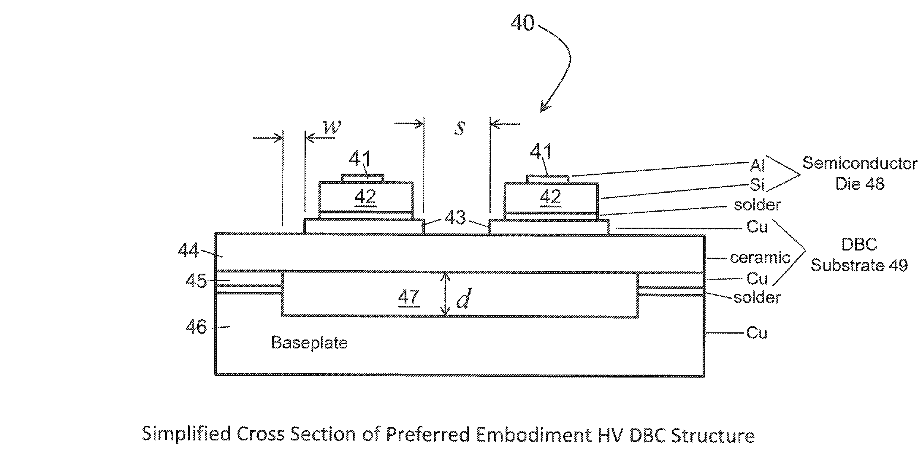
[0016]A preferred embodiment of the present invention comprises a novel packaging technique that enables the compact integration of state-of-the-art HV semiconductor devices. To realize the improved thermal performance of the planar packaging scheme with HV (>6-kV) die, electric fields must be mitigated in the ceramic portion of the substrate or substrates. To reduce the electric fields within the substrate(s) or substrate region(s), a preferred embodiment, as illustrated in FIG. 9, comprises a pocket 47 which may be cut in the metal baseplate 46 and the bottom direct bonded copper (DBC) layer 45. This “pocket” region is a dielectric region and may be filled with the ambient gas such as air, a liquid such as mineral oil, or a solid such as silicone, for example. The pocket may be patterned, for example, as shown in FIG. 9. The pocket depth (d), pad margin (w), and pad spacing (s) are adjusted to reduce electric field intensities. As an example, d=1.8 mm and w=s=2 mm. There are two regions of interest in this geometry: regions directly under the diode mounting pads (“A-regions”) and the inter-diode regions where there is no top metallization (“B-regions”). The maximum electric field in the A-regions is approximately 1.2 MV / m (a 92% reduction over the solid baseplate case), which is well below the partial discharge (PD) threshold of 7 MV / m. In the B-region, the maximum field intensity is approximately 8 MV / m. As the pocket depth is increased, the magnitude of the electric field in the B-regions decreases, as shown in FIG. 11. In this example, increasing the pocket depth more than 1 mm does not significantly reduce the electric field in these regions. The electric field intensity in the B-regions is, however, a strong function of the lateral separation and potential of the top metallization pads. This leads to a design trade-off between overall package size and component reliability. For the example design, FIG. 12 shows the dependence of electric field intensity within the AIN layer, as spacing s is varied from 0.5 to 4 mm with an applied potential difference of 15 kV. By increasing the pad spacing to 2 to 3 mm, one may operate below the PD threshold.
[0017]An aspect of the present invention is to effectively increase the dielectric strength of the substrate region under the die by introducing the dielectric region which is generally contiguous with the substrate region. The thickness of the substrate region (0.4 to 2 mm) and thickness of the dielectric region (0.2 to 4 mm) add to increase the distance between conducting surfaces thereby reducing the electric field (megavolts per meter) under the die. The dielectric region may be formed from dielectric materials which operate to increase the breakdown strength. Because DBC ceramic is generally only available up to thicknesses of 1 mm, the reduction of electric field required to quench partial discharge degradation usually not possible using only DBC. Furthermore, thick layers of DBC will have high thermal resistance which will reduce heat spreading and increase the temperature of the die. Therefore, the thicknesses of the dielectric and ceramic regions are critical parameters in the design of the present invention.
[0018]A preferred method of making an electronic device structure comprises providing at least one substrate region and providing at least one semiconductor die located on the at least one substrate region. Either (1) a portion of the at least one substrate region may be removed to provide a dielectric region within the at least one substrate region extending below the at least one semiconductor die; or (2) the at least one substrate may be produced or manufactured with a portion of the at least one substrate region comprising a dielectric region. The result produces a dielectric region which operates to reduce electric field stresses produced by the at least one semiconductor die to thereby reduce the possibility of material failure and voltage breakdown. For example, when using a direct bonded copper, direct bonded aluminum, or direct plated copper substrate in combination with a base plate comprising a metallic material, a capacitive effect is produced between the base plate and one of the direct bonded copper, direct bonded aluminum, or direct plated copper substrate region. Consequently, when a portion of the base region is removed to form the dielectric region, this operates to increase the distance between the resultant base plate and one of the direct bonded copper, direct bonded aluminum, or direct plated copper substrate. Of particular concern is the area underneath each of the semiconductor die. The preferred embodiment creates a dielectric region substantially underneath each of the semiconductor die while maintaining the mechanical strength in other areas.

