Check patentability & draft patents in minutes with Patsnap Eureka AI!

Method of forming mask pattern

a mask pattern and mask technology, applied in the field of mask pattern formation, can solve the problems of difficult to reduce the size of the opening portion by a slimming process or the like, the resolution of the micronization of recent semiconductor devices is better, and the number of processes is increasing

Active Publication Date: 2013-10-08
TOKYO ELECTRON LTD
View PDF3 Cites 2 Cited by
  • Summary
  • Abstract
  • Description
  • Claims
  • Application Information

AI Technical Summary

Benefits of technology

This approach reduces the number of processing steps and enhances the accuracy of pattern formation, allowing for the creation of features at or below the resolution limit of existing photolithography machines, thereby overcoming the limitations of traditional double patterning techniques.

Problems solved by technology

However, the micronization of recent semiconductor devices requires resolution better than the resolution limit of the photolithographic technique.
However, when the resist pattern is formed by double patterning such as the LELE process described above, the following problems may occur.
Therefore, there is a drawback that the number of processes increases.
However, when the resist pattern including the opening portions is formed, it is difficult to reduce the sizes of the opening portions by a slimming process or the like.
Thus, it is difficult to form opening portions having sizes of the resolution of the photolithography machine or smaller.[Patent Document 1] Japanese Laid-open Patent Publication No. 2005-129761

Method used


Image

  • Method of forming mask pattern
  • Method of forming mask pattern
  • Method of forming mask pattern

Examples


Embodiment Construction

[0024]A description is given below, with reference to the FIG. 1A through FIG. 7C of embodiments of the present invention.

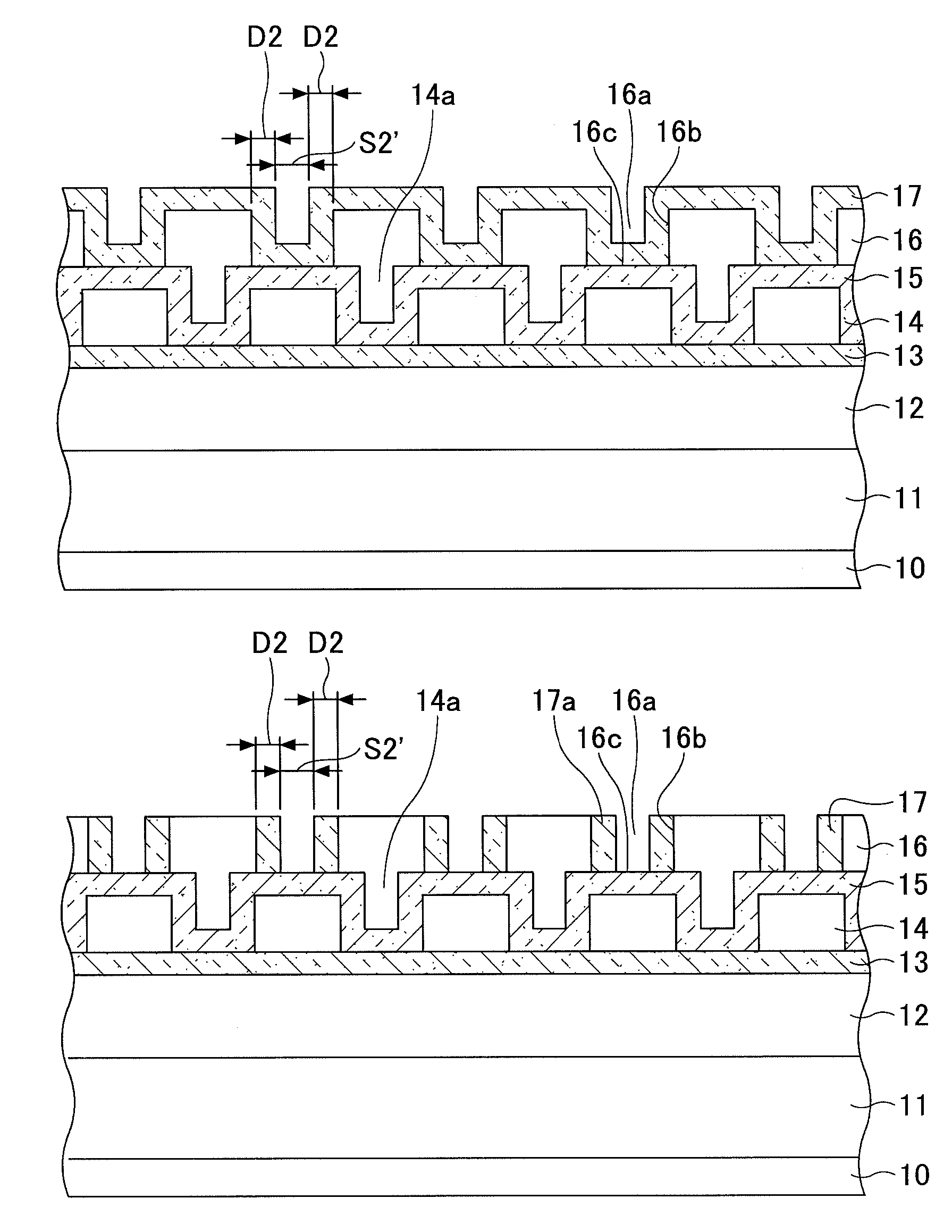
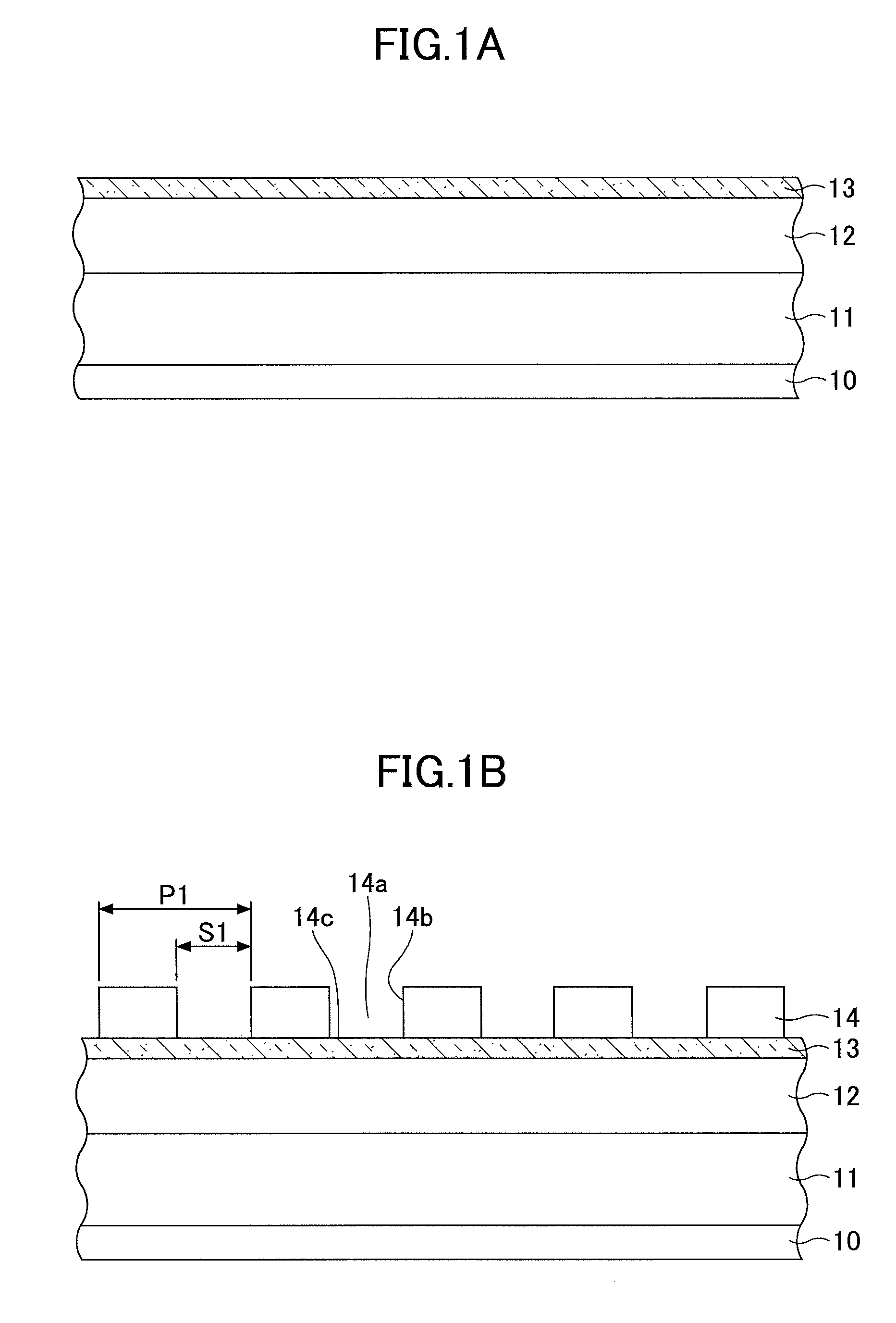
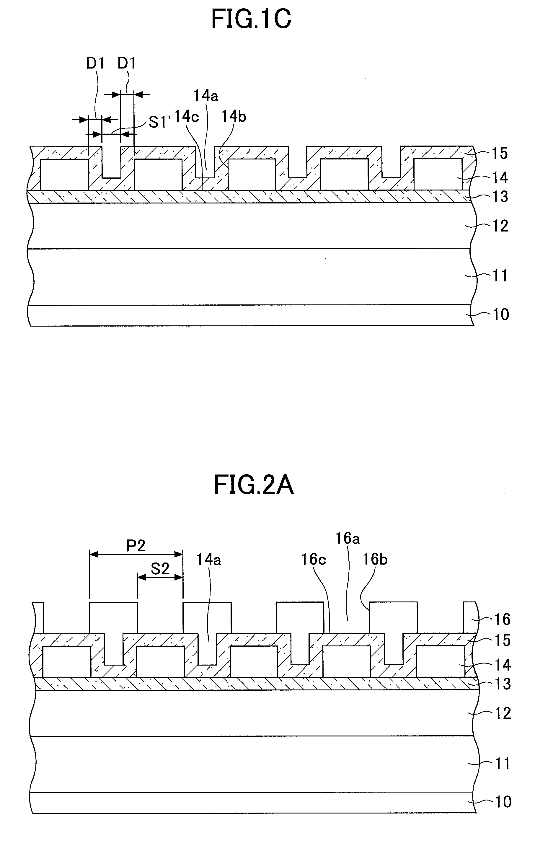
[0025]Hereinafter, reference symbols typically designate as follows:[0026]10: substrate;[0027]11: first film to be etched;[0028]12: second film to be etched;[0029]13: third film to be etched;[0030]14: first resist film;[0031]14a: first opening portion;[0032]14d: third opening portion;[0033]14g: fourth opening portion;[0034]15: first film;[0035]15a,17a: sidewall portion;[0036]16: second resist film;[0037]16a: second opening portion; and[0038]17: second film.

[0039]A description is given below, with reference to the FIG. 1 through FIG. 7 of embodiments of the present invention.

[0040]Referring to FIG. 1 to FIG. 5, a method of forming a mask pattern of an embodiment is described.

[0041]FIG. 1A to FIG. 4 are cross-sectional views schematically illustrating the structure of the substrate for explaining a method of forming a mask pattern of an embodiment. FIG. 5 is a plan...


PUM

PropertyMeasurementUnit
thicknessaaaaaaaaaa
thicknessaaaaaaaaaa
thicknessaaaaaaaaaa

Abstract

A disclosed method of forming a mask pattern includes forming a first resist film on a film to be etched, opening portions on the first resist film at a predetermined pitch, a first film on the first resist film so as to cover sidewalls of the first opening portions, a second resist film, second opening portions alternately arranged with the first opening portions on the second resist film, and a second film on the second resist film so as to cover sidewalls of the second opening portions, and removing a part of the second film so that the second film is left as first sidewall portions, a part of the first resist film using the first sidewall portions as a mask to form third opening portions, and a part of the first film while leaving the first film as second sidewall portions to form fourth opening portions.

Description

CROSS-REFERENCE TO RELATED APPLICATIONS[0001]This patent application is based upon and claims the benefit of priority of Japanese Patent Application No. 2011-025465 filed on Feb. 8, 2011, the entire contents of which are incorporated herein by reference.BACKGROUND OF THE INVENTION[0002]1. Field of the Invention[0003]The present invention generally relates to a method of forming a mask pattern on a substrate.[0004]2. Description of the Related Art[0005]Along with advances in a highly integrated circuit, wirings and separation widths required for the manufacturing process are being miniaturized. The micropattern is ordinarily formed by making a resist pattern using a photolithographic technique and etching various thin underlying films using the resist pattern as an etching mask. Therefore, in order to form the micropattern, the photolithographic technique is important. However, the micronization of recent semiconductor devices requires resolution better than the resolution limit of t...

Claims


Application Information

Patent Timeline
Patent Type & Authority Patents(United States)
IPC IPC(8): G03F7/26
CPCG03F7/0035G03F7/40H01L21/02164H01L21/02219H01L21/02274H01L21/0228H01L21/0276H01L21/0337H01L21/0338H01L21/31116H01L22/12H01L22/20H01L2924/0002H01L2924/00
Inventor YAEGASHI, HIDETAMI
Owner TOKYO ELECTRON LTD
Features
  • R&D
  • Intellectual Property
  • Life Sciences
  • Materials
  • Tech Scout
  • Unparalleled Data Quality
  • Higher Quality Content
  • 60% Fewer Hallucinations
Learn More