Semiconductor device and method of manufacturing the same

a technology of semiconductor devices and semiconductor elements, applied in semiconductor devices, semiconductor/solid-state device details, electrical apparatus, etc., can solve the problems of increasing production costs, disadvantageous less reliable of semiconductor elements, etc., and achieve the effect of improving the reliability of bonding and reducing the resistance of bonding

Active Publication Date: 2013-11-12
PANASONIC SEMICON SOLUTIONS CO LTD
View PDF12 Cites 0 Cited by
  • Summary
  • Abstract
  • Description
  • Claims
  • Application Information

AI Technical Summary

Benefits of technology

[0032]As has been discussed, terminals are divided into two along a common boundary, coatings most suitable for two conductive bonding materials to be used are exposed on the terminals, the most suitable one of the coatings is selected, and the corresponding conductive bonding material is bonded onto the coating. Thus it is possible to improve the reliability of bonding and easily reduce a bonding resistance while suppressing a decrease in the reliability of a semiconductor element.

Problems solved by technology

However, the semiconductor element 103 receives a stress at least twice because of heat and vibrations during ultrasonic bonding, so that the semiconductor element 103 disadvantageously becomes less reliable.
Moreover, the use of different kinds of conductive ribbons results in a complicated ultrasonic bonding process and a complicated device and equipment, disadvantageously increasing the production cost.

Method used


Image

  • Semiconductor device and method of manufacturing the same
  • Semiconductor device and method of manufacturing the same
  • Semiconductor device and method of manufacturing the same

Examples


first embodiment

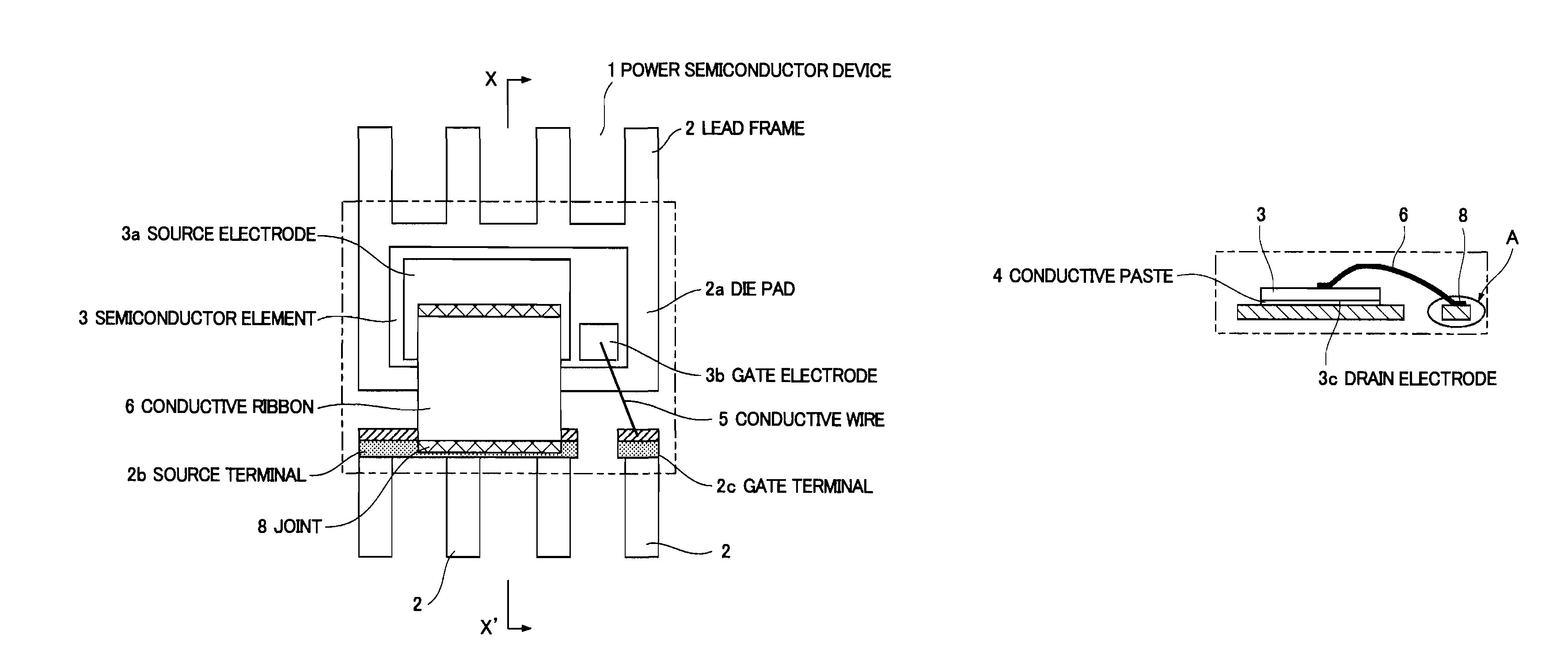
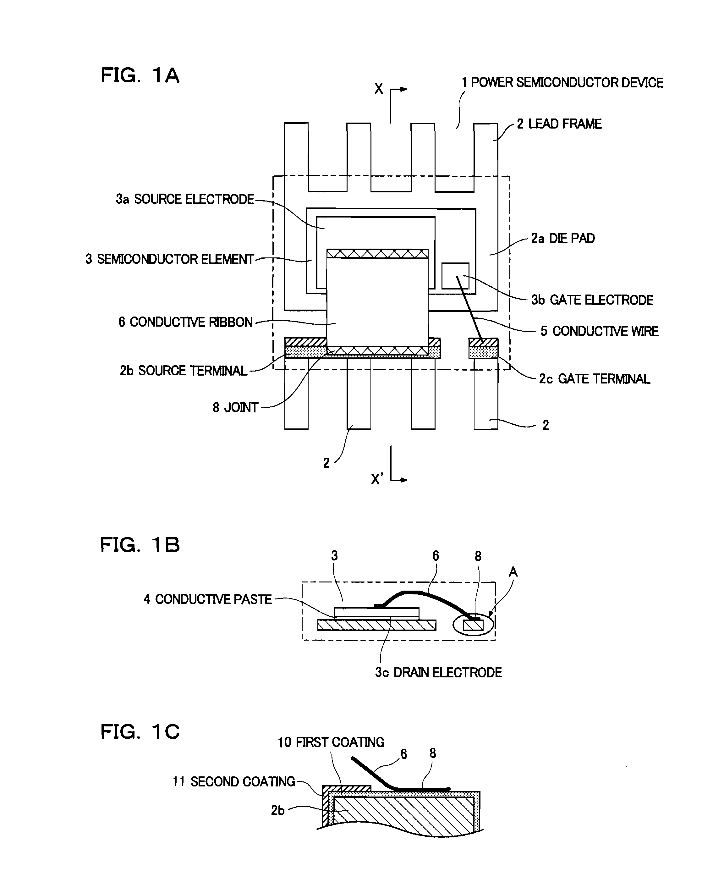
[0049]FIG. 1(a) is a plan view showing the configuration of a semiconductor device according to a first embodiment. The plan view shows the internal configuration of a MOS-FET that is a power semiconductor device. FIG. 1(b) is a sectional view showing the configuration of the semiconductor device according to the first embodiment, taken along line X-X′ of FIG. 1(a). FIG. 1(c) is an enlarged view showing the main part of the configuration of the coatings of the semiconductor device according to the first embodiment. FIG. 1(c) is also an enlarged view of part A of FIG. 1(b).

[0050]FIGS. 1(a) and 1(b) show a power semiconductor device 1 including a MOS-FET mounted as a semiconductor element 3 on a lead frame 2. On the major surface of the semiconductor element 3, a source electrode 3a and a gate electrode 3b are formed. The source electrode 3a and the gate electrode 3b are made up of conductive films, mainly Al films. The source electrode 3a is configured to have a larger area than the ...

second embodiment

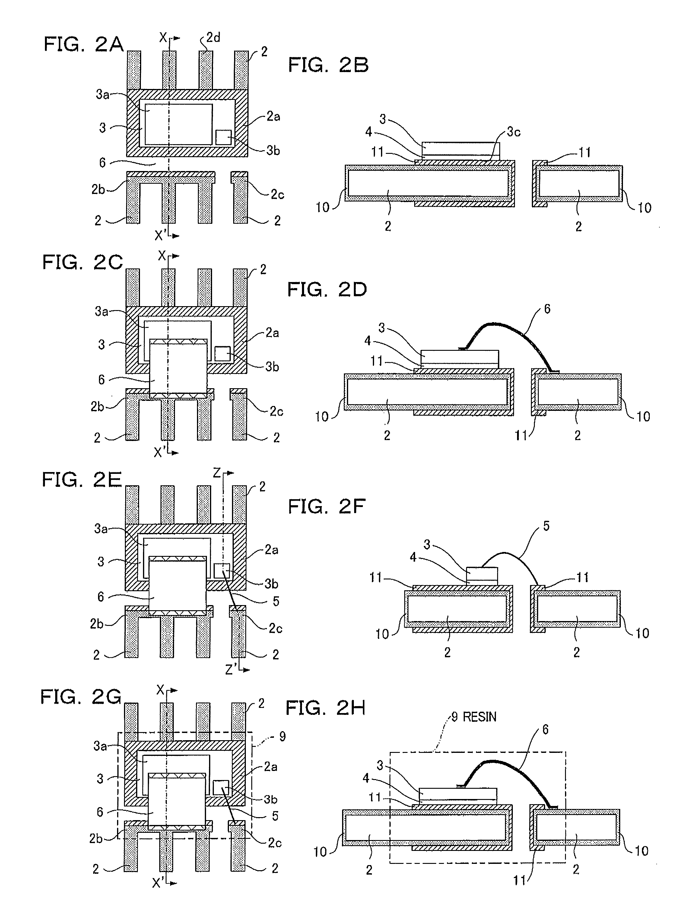
[0061]FIGS. 2(a), 2(c), 2(e), and 2(g) are process drawings showing a method of manufacturing a semiconductor device according to a second embodiment. FIGS. 2(b), 2(d), 2(f), and 2(h) are process drawings showing the method of manufacturing the semiconductor device according to the second embodiment. FIGS. 2(b), 2(d), 2(f), and 2(h) are sectional views taken along line X-X′ or Z-Z′ of FIGS. 2(a), 2(c), 2(e), and 2(g).

[0062]In FIGS. 2(a) to 2(h), a lead frame 2 is prepared that is made of copper or a copper alloy or an iron-nickel alloy. The lead frame 2 has a die pad 2a on which a semiconductor element 3 is placed; drain terminals 2d extended as second terminals from the die pad 2a; a source terminal 2b placed as a first terminal near the die pad 2a; and a gate terminal 2c serving as a third terminal. Further, Ag is applied as a first coating 10 over the surfaces of the source terminal 2b and the gate terminal 2c or at least on the outsides of the top surfaces of the source terminal...


PUM


Abstract

Terminals (2b, 2c) are divided into two along a common boundary, coatings (10, 11) most suitable for two conductive bonding materials (5, 6) to be used are exposed on the terminals (2b, 2c), the most suitable one of the coatings (10, 11) is selected, and the corresponding conductive bonding material (5, 6) is bonded onto the coating. Thus it is possible to improve the reliability of bonding and easily reduce a bonding resistance while suppressing a decrease in the reliability of a semiconductor element 3.

Description

TECHNICAL FIELD[0001]The present invention relates to a semiconductor device in which terminals are electrically connected via multiple kinds of conductive bonding materials, and a method of manufacturing the same.BACKGROUND ART[0002]There has been an increasing demand for higher power and a higher withstand voltage in lead frames and semiconductor devices of the prior art, e.g., power semiconductor devices in which power semiconductor elements such as a MOS-FET and an IGBT are mounted. Thus in some semiconductor elements and packages for the semiconductor elements in response to the demand, an electrical resistance at the joint of the semiconductor element and an external terminal is reduced by a strip of Al (aluminum ribbon) to apply a large current with a low resistance. In order to further reduce a resistance and improve connection stability, however, multiple Al ribbons are connected in a stacked manner with an increased cross sectional area.[0003]FIGS. 3(a) to 3(c) show the co...

Claims


Application Information

Patent Timeline
Patent Type & Authority Patents(United States)
IPC IPC(8): H01L23/495
CPCH01L23/49524H01L23/49582H01L24/06H01L24/37H01L24/40H01L24/73H01L24/83H01L23/49562H01L2924/1305H01L24/29H01L24/45H01L24/48H01L24/85H01L2224/04042H01L2224/05599H01L2224/0603H01L2224/29339H01L2224/32245H01L2224/45124H01L2224/45139H01L2224/45144H01L2224/48091H01L2224/48108H01L2224/48247H01L2224/48472H01L2224/73219H01L2224/73265H01L2224/8388H01L2224/85399H01L2224/85439H01L2224/85447H01L2224/85455H01L2224/92H01L2224/92247H01L2924/01004H01L2924/01013H01L2924/01029H01L2924/01047H01L2924/01078H01L2924/01079H01L2924/01082H01L2924/014H01L2924/0781H01L2924/13055H01L2924/13091H01L2924/1306H01L2224/40247H01L2924/01005H01L2924/01006H01L2924/01033H01L2924/00014H01L2924/01028H01L2224/48599H01L2224/48699H01L2224/73221H01L2224/83H01L2224/84H01L2224/85H01L2924/00H01L2924/00012H01L2924/351H01L2224/48639H01L2924/181H01L2224/48647H01L2224/48655H01L2224/48739H01L2224/48747H01L2224/48755H01L2224/40245H01L2224/40091H01L2924/00011H01L2224/05553H01L2224/05554H01L2224/37124H01L2224/8485H01L24/84H01L2924/01049H01L2224/45015H01L2924/207
Inventor YOKOE, TOSHIYUKIFUJIOKA, CHIEKUMANO, DAICHI
Owner PANASONIC SEMICON SOLUTIONS CO LTD
Why Eureka
Try Eureka