

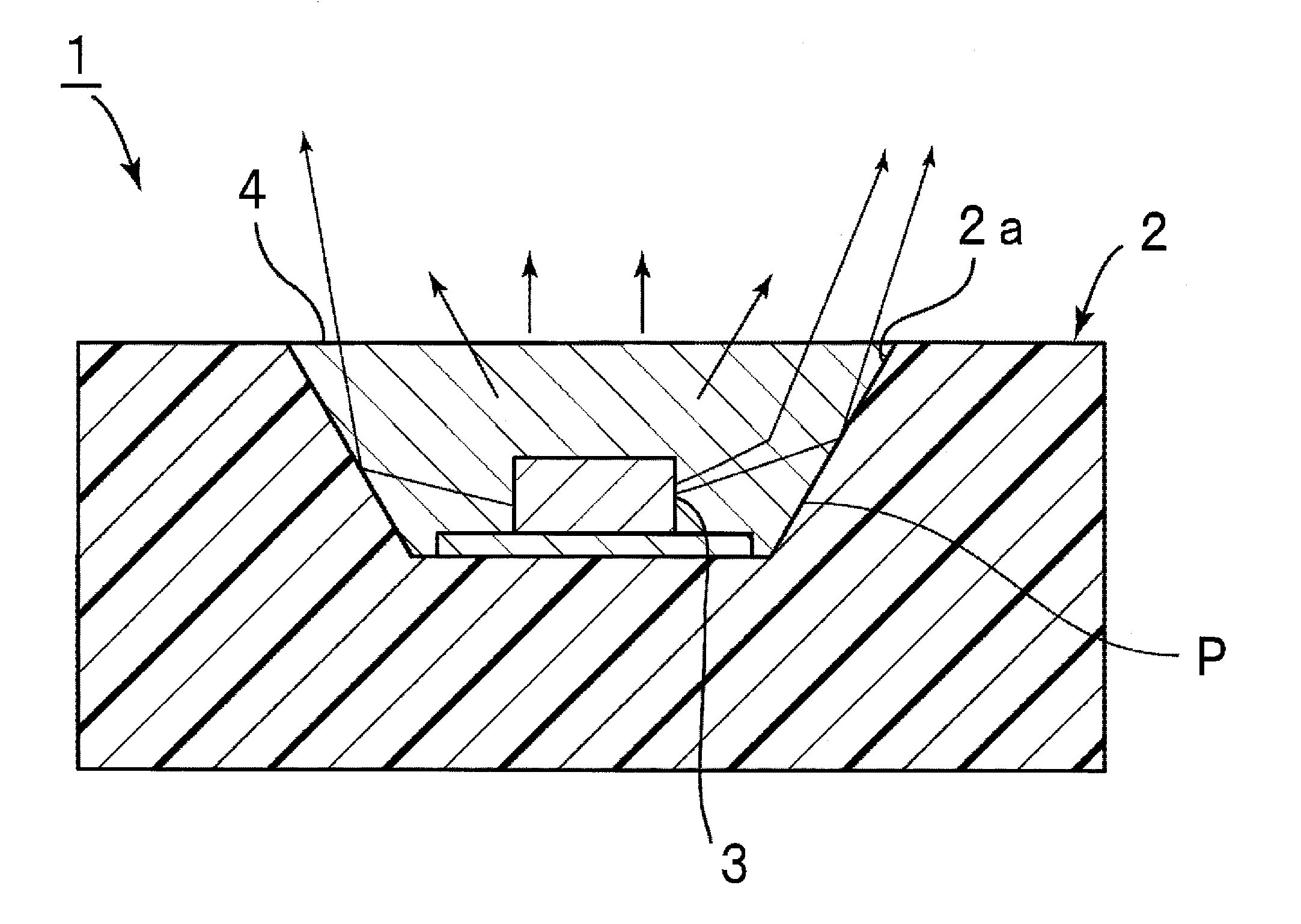
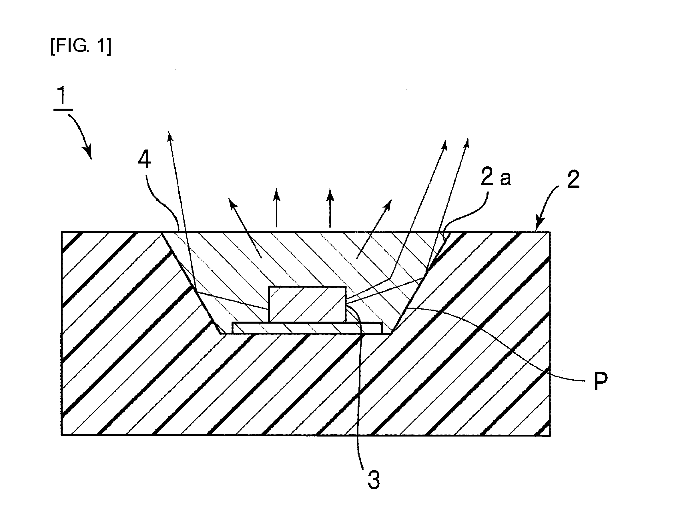
Encapsulating agent for optical semiconductor devices, and optical semiconductor device using same
a technology of optical semiconductor and encapsulating agent, which is applied in the direction of semiconductor/solid-state device details, other chemical processes, non-metal conductors, etc., can solve the problems of low power consumption of devices such as light emitting diodes (led) and a long lifetime, and achieve the effect of enhancing the adhesion between the housing and the encapsulant and enhancing the reliability of bonding
- Summary
- Abstract
- Description
- Claims
- Application Information
AI Technical Summary
Benefits of technology
Problems solved by technology
Method used
Image

Examples
synthesis example 1
Synthesis of First Organopolysiloxane
[0186]Into a 1000 mL separable flask equipped with a thermometer, a dropping device and a stirrer were added 63 g of trimethylmethoxysilane, 90 g of dimethyldimethoxysilane, 183 g of diphenyldimethoxysilane and 133 g of vinyltrimethoxysilane, and the mixture was stirred at 50° C. A solution obtained by dissolving 0.8 g of potassium hydroxide in 114 g of water was slowly added dropwise therein, and thereafter the mixture was stirred at 50° C. for 6 hours and reacted to obtain a reaction liquid. Next, 0.9 g of acetic acid was added to the reaction liquid, the pressure was reduced to remove volatile components, and potassium acetate was removed by filtration to obtain a polymer (A).
[0187]The number average molecular weight (Mn) of the obtained polymer (A) was 1700. The chemical structure was identified by 29Si-NMR, and resultantly it was found that the polymer (A) had the following average composition formula (A1).
(Me3SiO1 / 2)0.19(Me2SiO2 / 2)0.24(Ph2S...
synthesis example 2
Synthesis of First Organopolysiloxane
[0190]Into a 1000 mL separable flask equipped with a thermometer, a dropping device and a stirrer were added 96 g of dimethyldimethoxysilane, 318 q of diphenyldimethoxysilane and 119 g of vinylmethyldimethoxysilane, and the mixture was stirred at 50° C. A solution obtained by dissolving 0.8 g of potassium hydroxide in 108 g of water was slowly added dropwise therein, and thereafter the mixture was stirred at 50° C. for 6 hours and reacted to obtain a reaction liquid. Next, 0.9 g of acetic acid was added to the reaction liquid, the pressure was reduced to remove volatile components, and potassium acetate was removed by filtration to obtain a polymer (B).
[0191]The number average molecular weight (Mn) of the obtained polymer (B) was 5300. The chemical structure was identified by 29Si-NMR, and resultantly it was found that the polymer (B) had the following average composition formula (B1).
(Me2SiO2 / 2)0.25(Ph2SiO2 / 2)0.45(ViMeSiO2 / 2)0.30 formula (B1)
[0...
synthesis example 3
Synthesis of First Organopolysiloxane
[0193]Into a 1000 mL separable flask equipped with a thermometer, a dropping device and a stirrer were added 6.3 g of trimethylmethylmethoxysilane, 89 g of dimethyldimethoxysilane, 318 g of diphenyldimethoxysilane and 119 g of vinylmethyldimethoxysilane, and the mixture was stirred at 50° C. A solution obtained by dissolving 0.8 g of potassium hydroxide in 107 g of water was slowly added dropwise therein, and thereafter the mixture was stirred at 50° C. for 6 hours and reacted to obtain a reaction liquid. Next, 0.9 g of acetic acid was added to the reaction liquid, the pressure was reduced to remove volatile components, and potassium acetate was removed by filtration to obtain a polymer (C).
[0194]The number average molecular weight (Mn) of the obtained polymer (C) was 5000. The chemical structure was identified by 29Si-NMR, and resultantly it was found that the polymer (C) had the following average composition formula (C1).
(Me3SiO1 / 2)0.01(Me2SiO2...
PUM
| Property | Measurement | Unit |
|---|---|---|
| weight | aaaaa | aaaaa |
| molecular weight | aaaaa | aaaaa |
| power consumption | aaaaa | aaaaa |
Abstract
Description
Claims
Application Information