Wiring board and method of manufacturing the same

a technology of wiring board and manufacturing method, which is applied in the direction of paper/cardboard containers, electrical apparatus construction details, semiconductor/solid-state device details, etc., can solve the problems of increasing manufacturing costs, reducing the reliability of bonding large gap between the upper and lower packages, so as to improve the reliability of bonding and the effect of easy pop bonding

Active Publication Date: 2011-11-29
SHINKO ELECTRIC IND CO LTD
View PDF6 Cites 17 Cited by
  • Summary
  • Abstract
  • Description
  • Claims
  • Application Information

AI Technical Summary

Benefits of technology

[0014]An object of the present invention is to provide a wiring board which enables easier POP bonding with low costs and which achieves an improvement in the reliability of the bonding while contributing to making a smaller and thinner structure, and a method of manufacturing the same.
[0016]With the method of manufacturing a wiring board according to this aspect, in the wiring board to be obtained eventually, a cavity is formed at a position corresponding to an electronic component mounting area of the outermost insulating layer (for example, resin layer), the first pad is exposed from the surface of the insulating layer in the cavity, and the second pad is also exposed from the surface of the insulating layer in the peripheral region of the cavity. Specifically, the surface of the insulating layer from which the first pad is exposed is formed at a lower position than the surface of the insulating layer from which the second pad is exposed. Accordingly, POP bonding can be easily performed by using the second pad arranged in the peripheral region of the cavity as a terminal for POP bonding.
[0017]Namely, an electronic component (such as a semiconductor chip) mounted on the wiring board can be placed within the cavity, so that the gap between the present package and another package bonded to the second pad in the peripheral region of the cavity can be made relatively narrow. Thus, without placing the interposer such as employed in the prior art, the upper and lower packages can be easily bonded via a small amount of solder (solder bump or the like) in accordance with the gap which is made narrow. Consequently, since no interposer is needed in performing POP bonding, a reduction in cost can be achieved.
[0018]Moreover, the amount of use of the solder (bump) for bonding the upper and lower packages can be less when performing POP bonding, so that the inconveniences (separation of solder, formation of a bridge and the like) such as encountered in the prior art can be removed. This advantage contributes to an improvement in the reliability of the bonding.
[0019]Furthermore, since the electronic component to be mounted can be placed within the cavity, the height of the wiring board can be made relatively small, which in turn contributes to making a smaller and thinner structure. As a result, it becomes possible to achieve a desired smaller and thinner structure in implementing a POP structure.
[0021]With the method of manufacturing a wiring board according to this aspect, since the wiring board to be eventually obtained has the same structure, the same operational effects can be brought about as in the case of the method of manufacturing a wiring board according to the aforementioned aspect.

Problems solved by technology

However, in the case where an interposer is used for bonding, there arises a problem in that another process (considerable manufacturing steps) for fabricating the interposer is required, and a material for fabricating the interposer is required as well, to thus increase the manufacturing cost.
On the other hand, in the case where solder is used for bonding, the gap between the upper and lower packages is large because of the presence of the chip mounted between the packages.
In this case, there are inconveniences such as separation of the bump (solder) during reflow soldering, and formation of a bridge between adjacent bumps.
This leads to a problem in that the reliability of bonding between the upper and lower packages decreases.
In addition, because of the presence of the chip mounted between the upper and lower packages, both of the above bonding methods have another problem in that, where the chip has a large thickness, the whole POP structure cannot be constructed as small and thin as desired.

Method used


Image

  • Wiring board and method of manufacturing the same
  • Wiring board and method of manufacturing the same
  • Wiring board and method of manufacturing the same

Examples


first embodiment

; See FIGS. 1 to 6

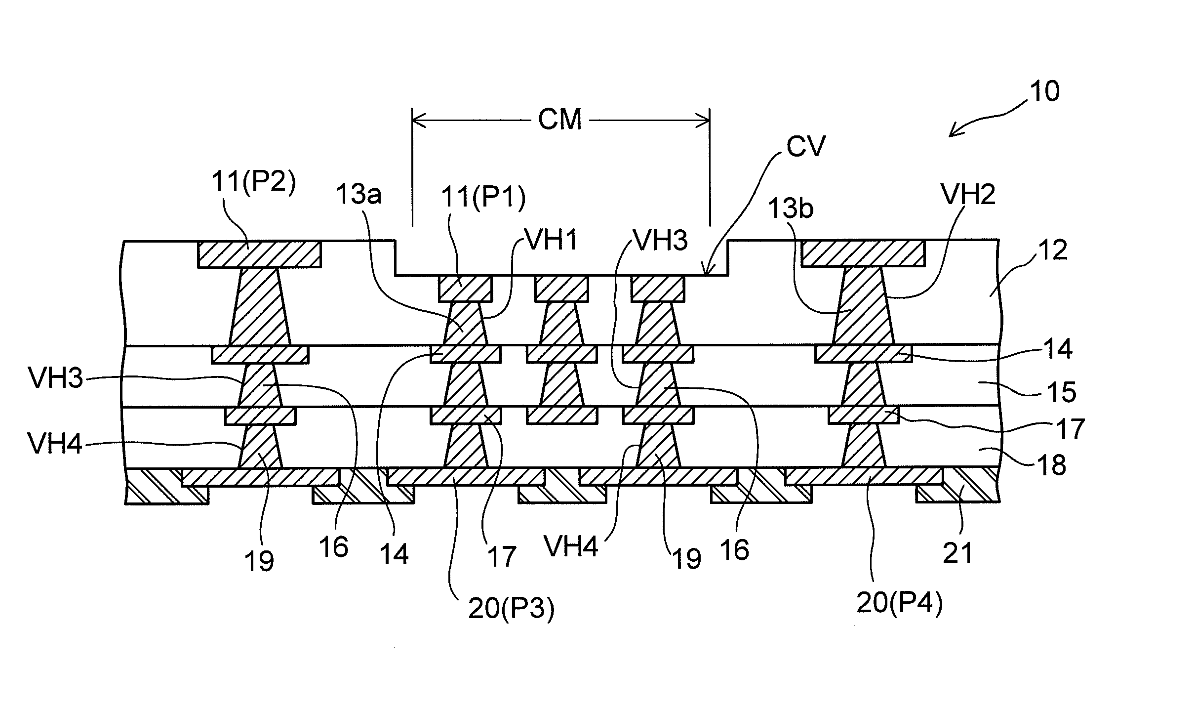
[0032]FIG. 1 shows a configuration of a wiring board (semiconductor package) according to a first embodiment of the present invention, in the form of a cross-sectional view.

[0033]The wiring board (semiconductor package) 10 according to the present embodiment has a structure in which a plurality of wiring layers 11, 14, 17 and 20 are stacked one on top of another with insulating layers (specifically, resin layers) 12, 15 and 18 interposed between corresponding wiring layers, as illustrated. In this structure, the wiring layers 11, 14, 17 and 20 are connected via conductors (vias 13a and 13b, 16 and 19), respectively, filled into via holes VH1 and VH2, VH3 and VH4 each formed in a corresponding one of the insulating layers 12, 15 and 18. Namely, the package 10 has the form of a “coreless substrate,” which does not include a support base member, and is different from a wiring board fabricated by using a general build-up process (in which a required number of build-up ...

second embodiment

; See FIG. 7

[0084]FIG. 7 shows a configuration of a wiring board (semiconductor package) according to a second embodiment of the present invention, in the form of a cross-sectional view.

[0085]As compared with the configuration of the wiring board 10 (FIG. 1) according to the first embodiment, the wiring board (semiconductor package) 10a according to the second embodiment is different in that the pads P1 arranged in the chip mounting area CM in the cavity CV are formed in a way that the surfaces of the pads P1 are located at a position recessed from the bottom surface (surface of the resin layer 12a) of the cavity CV to the inner side of the board by a predetermined depth. Specifically, recessed portions DP are formed at positions corresponding to the pads P1, respectively, on the resin layer 12a in the cavity CV. Since the other configuration of the wiring board 10a is basically the same as that of the wiring board 10 in FIG. 1, the description thereof is omitted herein.

[0086]The wi...

third embodiment

; See FIG. 8

[0094]FIG. 8 shows a configuration of a wiring board (semiconductor package) according to a third embodiment of the present invention, in the form of a cross-sectional view.

[0095]As compared with the configuration of the wiring board 10 (FIG. 1) according to the first embodiment, the wiring board (semiconductor package) 10b according to the third embodiment is different in the following points. First, the pads P1 arranged in the chip mounting area CM in the cavity CV are formed in a way that the surfaces of the pads P1 are located at a position recessed from the bottom surface (surface of the resin layer 12) of the cavity CV to the inner side of the board by a predetermined depth. Moreover, the pads P2 arranged in the peripheral region of the cavity CV are formed in a way that the surfaces of the pads P2 are located at a position recessed to the inner side of the board from the surface of the resin layer 12b by a predetermined depth. Specifically, recessed portions DP1 a...


PUM

PropertyMeasurementUnit
diameteraaaaaaaaaa
sizeaaaaaaaaaa
thicknessaaaaaaaaaa

Abstract

A wiring board (package) includes: a cavity formed at a position corresponding to a chip mounting area of the outermost insulating layer on one side of both surfaces of the wiring board; a pad exposed from the surface of the insulating layer in the cavity; and a pad exposed from the surface of the insulating layer in a peripheral region of the cavity. A chip is flip-chip bonded to the pads in the cavity of the package, and another package is bonded to the pads in the peripheral region of the cavity, to thereby form a semiconductor device having a package on package (POP) structure.

Description

CROSS-REFERENCE TO RELATED APPLICATIONS[0001]This application is based on and claims priority of Japanese Patent Application No. 2008-317410 filed on Dec. 12, 2008, the entire contents of which are incorporated herein by reference.BACKGROUND OF THE INVENTION[0002](a) Field of the Invention[0003]The present invention relates to a wiring board and a method of manufacturing the same. More specifically, the invention relates to a wiring board having a structure in which terminals (pads) for mounting a semiconductor element (chip) or the like or for external connection are exposed from an outermost insulating layer, and also to a method of manufacturing the same.[0004]In the description below, the wiring board is also referred to as a “semiconductor package” for the sake of convenience.[0005](b) Description of the Related Art[0006]In a trend to make semiconductor devices smaller (thinner) in size and higher in performance (function), there is a demand for package-on-package (POP) bonding...

Claims


Application Information

Patent Timeline
Patent Type & Authority Patents(United States)
IPC IPC(8): H05K1/00
CPCH01L23/13H01L25/105H05K3/4697H01L23/49822Y10T156/10H01L23/49827H01L23/50H01L2224/16225H01L2224/73204H01L2924/01046H01L2924/01078H01L2924/01079H01L2924/15311H01L2924/15331H01L2924/19041H01L2924/19105H01L2924/19106H05K1/183H05K3/205H05K3/4682H05K2201/09472H05K2201/09481H05K2201/10674H05K2203/0369H05K2203/0376H01L2924/3511H01L2225/1058H01L2224/32225H01L2924/00012H01L2924/00
Inventor KANEKO, KENTARO
Owner SHINKO ELECTRIC IND CO LTD
Why Eureka
Try Eureka