Image processing circuit and associated method

a technology of image processing and circuit, applied in the field of image processing mechanism, can solve the problems of increasing circuit cost as a whole and lowering overall performance, and achieve the effect of increasing circuit cost, reducing line buffer storage volume and associated methods

Active Publication Date: 2013-11-12
MEDIATEK INC
View PDF13 Cites 2 Cited by
  • Summary
  • Abstract
  • Description
  • Claims
  • Application Information

AI Technical Summary

Benefits of technology

[0005]Therefore, to, among other things, overcome the foregoing issue of increased circuit cost, the present invention provides an image processing circuit capable of reducing a storage volume of line buffers and an associated method.

Problems solved by technology

Supposing the motion estimation / compensation circuit frequently accesses the DRAM for the source image data, an overall performance is lowered due to latencies of the DRAM.
However, when there are a large number of line buffers or when an overall storage volume needed by the line buffers is large, circuit cost as a whole is increased.

Method used


Image

  • Image processing circuit and associated method
  • Image processing circuit and associated method
  • Image processing circuit and associated method

Examples


Embodiment Construction

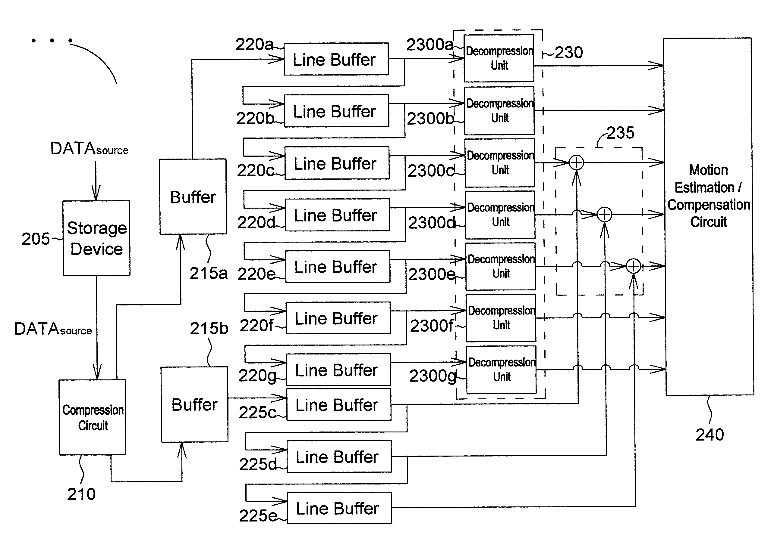
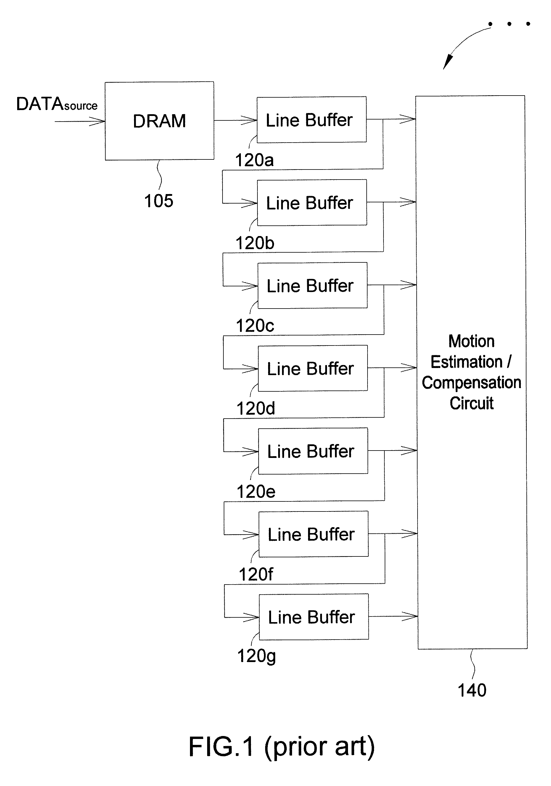
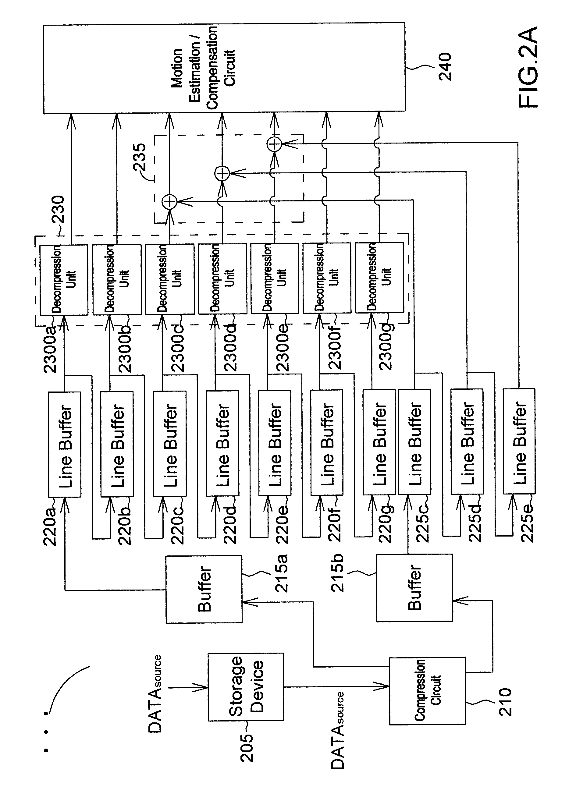
[0014]FIG. 2A shows a block diagram of an image processing circuit 200 according to one preferred embodiment of the invention, and FIG. 2B shows a flowchart of operating the image processing circuit 200 in FIG. 2A. The image processing circuit 200 comprises a storage device 205, a compression circuit 210, two buffers 215a and 215b, a first plurality of line buffers 220a˜220g, a second plurality of line buffers 225c˜225e, a decompression circuit 230, a processing circuit 235, and a motion estimation / compensation circuit 240. The storage device 205 may be a DRAM. The line buffers 220a˜220g, and 225c˜225e may be an SRAM. The image processing circuit 200 may be designed as a single chip, or the storage device 205 may be designed as a DRAM chip independent from the image processing circuit 200. As shown in FIG. 2B, in step 405, the storage device 205 stores source image data DATAsource inputted into the image processing circuit 200. In step 410, the compression circuit 210 receives the s...


PUM


Abstract

An image processing circuit includes a compression circuit, a plurality of first line buffers, a decompression circuit, and a motion estimation / compensation circuit. The compression circuit receives source image data and compresses the received source image data to generate a compressed image data. The first line buffers, coupled to the compression circuit, sequentially receive the compressed image data and buffer the compressed image data. The decompression circuit, coupled to the first line buffers, decompresses the compressed image data to generate a decompressed image data. The motion estimation / compression circuit, coupled to the decompression circuit, performs motion estimation / compensation according to the decompressed image data.

Description

CROSS REFERENCE TO RELATED PATENT APPLICATION[0001]This patent application is based on Taiwan, R.O.C. patent application No. 097123113 filed on Jun. 20, 2008.FIELD OF THE INVENTION[0002]The present invention relates to an image processing mechanism, and more particularly, to an image processing circuit capable of reducing a total volume of line buffers and an associated method.BACKGROUND OF THE INVENTION[0003]In image processing, a dynamic random access memory (DRAM) is commonly used for storing source image data, which is then used for image processing when a subsequent motion estimation / compensation circuit accesses the DRAM. Note that a bandwidth of the DRAM is rather valuable. Supposing the motion estimation / compensation circuit frequently accesses the DRAM for the source image data, an overall performance is lowered due to latencies of the DRAM. Therefore, the prior art provides a plurality of line buffers between the DRAM and the motion estimation / compensation circuit, wherein...

Claims


Application Information

Patent Timeline
Patent Type & Authority Patents(United States)
IPC IPC(8): H04N11/02
CPCH04N19/43H04N19/436
Inventor CHEN, CHUNG-YIWANG, SU-CHUN
Owner MEDIATEK INC
Why Eureka
Try Eureka