
Reconfigurable logic block, programmable logic device provided with the reconfigurable logic block, and method of fabricating the reconfigurable logic block

a programmable logic and reconfigurable logic technology, applied in the field of reconfigurable logic blocks, can solve the problems of reducing the area efficiency of the chip, reducing the efficiency of the implementation, and reducing the area efficiency of the device, so as to achieve the effect of high area efficiency of the chip, low power consumption, and high speed

Inactive Publication Date: 2013-11-19
SEMICON TECH ACADEMIC RES CENT
View PDF22 Cites 7 Cited by
  • Summary
  • Abstract
  • Description
  • Claims
  • Application Information

AI Technical Summary

Benefits of technology

[0018]An object of the present invention is to maintain a high area efficiency of a chip, regardless of a circuitry configured therein, and aim for both a higher speed and a lower low power consumption.

Problems solved by technology

As described above, since a prior-art device such as an FPGA based on a fine-grained LUT is inferior for implementing an arithmetic circuit, another component such as a multiplier is mounted separately, and thus the area efficiency (implementation efficiency) of the chip is reduced by that amount.
Similarly, a device such as a DRP or DAP / DNA based on a coarse-grained type ALU has a bad area efficiency when used to configure a random logic (glue logic) circuit.
More specifically, any deterioration of capabilities is avoided by having an arithmetic-logic unit that is called a data management unit (DMU) in addition to the ALU, but if this arithmetic-logic unit is not used, that in itself will be a cause of a drop in area efficiency.
This makes it impossible to prevent deterioration in the area efficiency of the chip.
More specifically, since an adder circuit of the operation cell disclosed in Japanese Unexamined Patent Publication (Kokai) No. 10-111790 is configured of an two 8-LUTs, by way of example, and the two LUTs are not connected internally, the original capability thereof as an adder is insufficient from the viewpoints of both area efficiency and speed.
In addition, since each RLB of the operation cell disclosed in Japanese Unexamined Patent Publication (Kokai) No. 10-111790 is configured of two 8-LUTs during logical operations, the area efficiency thereof is even worse.
The programmable function block disclosed in Japanese Unexamined Patent Publication (Kokai) No. 11-024891 by way of example is provided with a one-bit full adder and front logic within each RLB, but since carries are through external wiring during operations with a plurality of bits, problems arise in that speed overheads increase and completion of the logic cannot be ensured during logical operations.

Method used


Image

  • Reconfigurable logic block, programmable logic device provided with the reconfigurable logic block, and method of fabricating the reconfigurable logic block
  • Reconfigurable logic block, programmable logic device provided with the reconfigurable logic block, and method of fabricating the reconfigurable logic block
  • Reconfigurable logic block, programmable logic device provided with the reconfigurable logic block, and method of fabricating the reconfigurable logic block

Examples


Embodiment Construction

[0055]Below, embodiments of a reconfigurable logic block (RLB), a programmable logic device having the RLB, and a method of fabricating the RLB in accordance with the present invention will be described in detail with reference to the accompanying drawings.

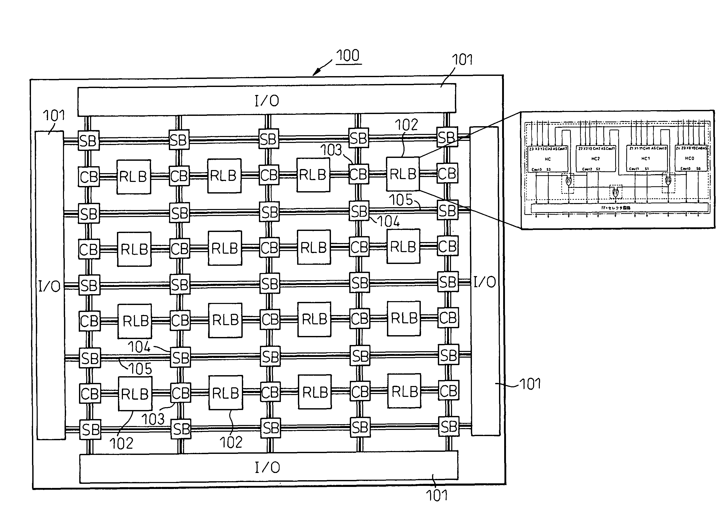
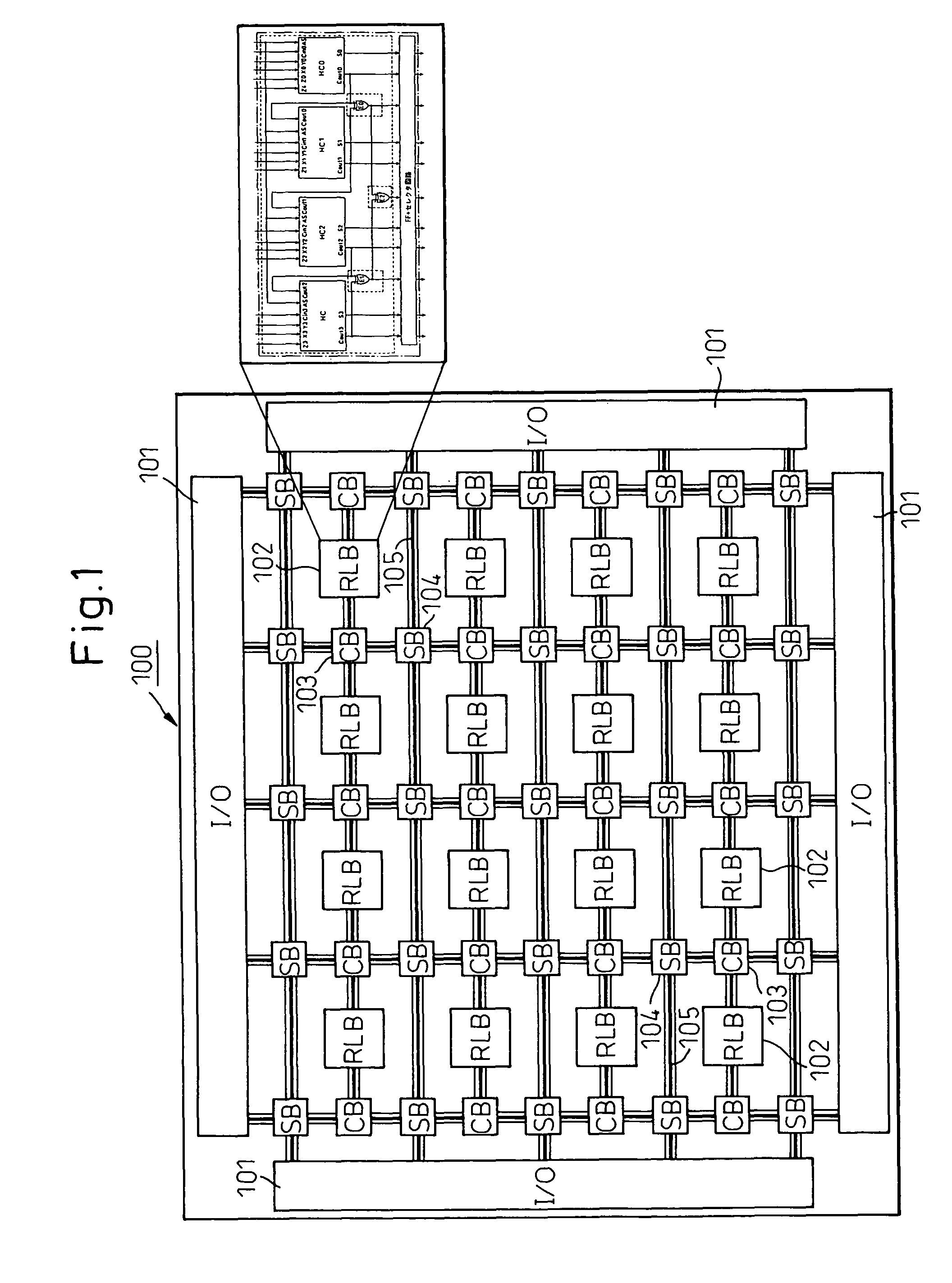
[0056]A block diagram of the entire configuration of a programmable logic device in which the present invention is used is shown in FIG. 1. In FIG. 1, reference number 100 denotes a programmable logic device, 101 denotes an input / output block (I / O block), 102 denotes an RLB, 103 denotes a connection block (CB), 104 denotes a switch block (SB), and 105 denotes wiring.

[0057]As shown in FIG. 1, the programmable logic device 100 is provided with a plurality of RLBs 102 arrayed in a matrix, CBs 103 that link each RLB 102 to the wiring 105, an SB 104 formed at each crossing point of the wiring 105, and I / O blocks 101 that input and output signals with respect to the exterior. Note that the present invention mainly relates to the configu...


PUM


Abstract

A reconfigurable logic block has a first circuit that configures an arithmetic circuit and a second circuit that configures a circuit outside of the arithmetic circuit. A plurality of different circuits are configured by changing the settings of predetermined signals in the first and second circuits.

Description

CROSS REFERENCE TO RELATED APPLICATION[0001]This application is based upon and claims the benefit of priority from, the prior Japanese Patent Application Nos. 2005-330268 filed on Nov. 15, 2005 and 2006-166387 filed on Jun. 15, 2006, the entire contents of which are incorporated herein by reference.BACKGROUND OF THE INVENTION[0002]1. Field of the Invention[0003]The present invention relates to a reconfigurable logic block (RLB), a programmable logic device that is provided with an RLB, and a method of fabricating an RLB, and, in particular, to a technique of fabricating an RLB that enables a reduction in implementation area.[0004]2. Description of the Related Art[0005]Programmable logic devices have recently attracted attention as devices that a user can use to implement logic circuits to suit various different requirements, by electrically programming the internal circuitry thereof. Programmable logic devices (PLDs), field programmable gate arrays (FPGAs), dynamically reconfigurabl...

Claims


Application Information

Patent Timeline
Patent Type & Authority Patents(United States)
IPC IPC(8): H03K19/173
CPCH03K19/17728H03K19/17748
Inventor SUEYOSHI, TOSHINORIIIDA, MASAHIROAMAGASAKI, MOTOKITAKETA, KAZUHIKOHEISHI, TAKETOSUZUKI, NOBUHARU
Owner SEMICON TECH ACADEMIC RES CENT
Learn More