Programmable logic device and semiconductor device

Active Publication Date: 2013-11-28
SEMICON ENERGY LAB CO LTD
View PDF13 Cites 75 Cited by
  • Summary
  • Abstract
  • Description
  • Claims
  • Application Information

AI Technical Summary

Benefits of technology

[0034]In the configuration memory in the third embodiment, a portion configured with the first and second switches and a portion configured with the third and fourth switches have the same connection structure between the switches as a portion configured with the first and second switches in the switch circuit of the second embodiment. Accordingly, in the fourth embodiment of the present invention, the configuration memories and the switch circuits are arranged in rows and columns, so that the operation of the configuration memories and the operation of the switch circuits can be controlled by the same driver circuit. Thus, an increase in the area of a programmable logic device can be prevented as compared to the case where a driver circuit for the switch circuits and a driver circuit for the configuration memories are separately provided.
[0035]One embodiment of the present invention can provide a programmable logic device in which the area of a storage device is small. One embodiment of the present invention can provide a programmable logic device in which a logic circuit can be reconfigured at high speed an

Problems solved by technology

Since a PLD employing a multi-context system needs to have a configuration memory in addition to a memory element, the area of storage devices such as the memory element and the configuration memory in the PLD is larger than in the case of using another method of performing dynamic reconfiguration, such as a configuration data transfer method, and thus the PLD cannot fully take advantage of high area efficiency of dynamic reconfiguration.
In particular, an SRAM requires a large number of elements per memory cell; thus, it is difficult to keep the area of storage devices small.
A DRAM has a smaller number of elements per memory cell than an SRAM and is effective in keeping the area of a storage device small; however, it is difficult to reduce power consumption because refresh operation is necessary.
As a result, it takes time to

Method used


Image

  • Programmable logic device and semiconductor device
  • Programmable logic device and semiconductor device
  • Programmable logic device and semiconductor device

Examples


Embodiment Construction

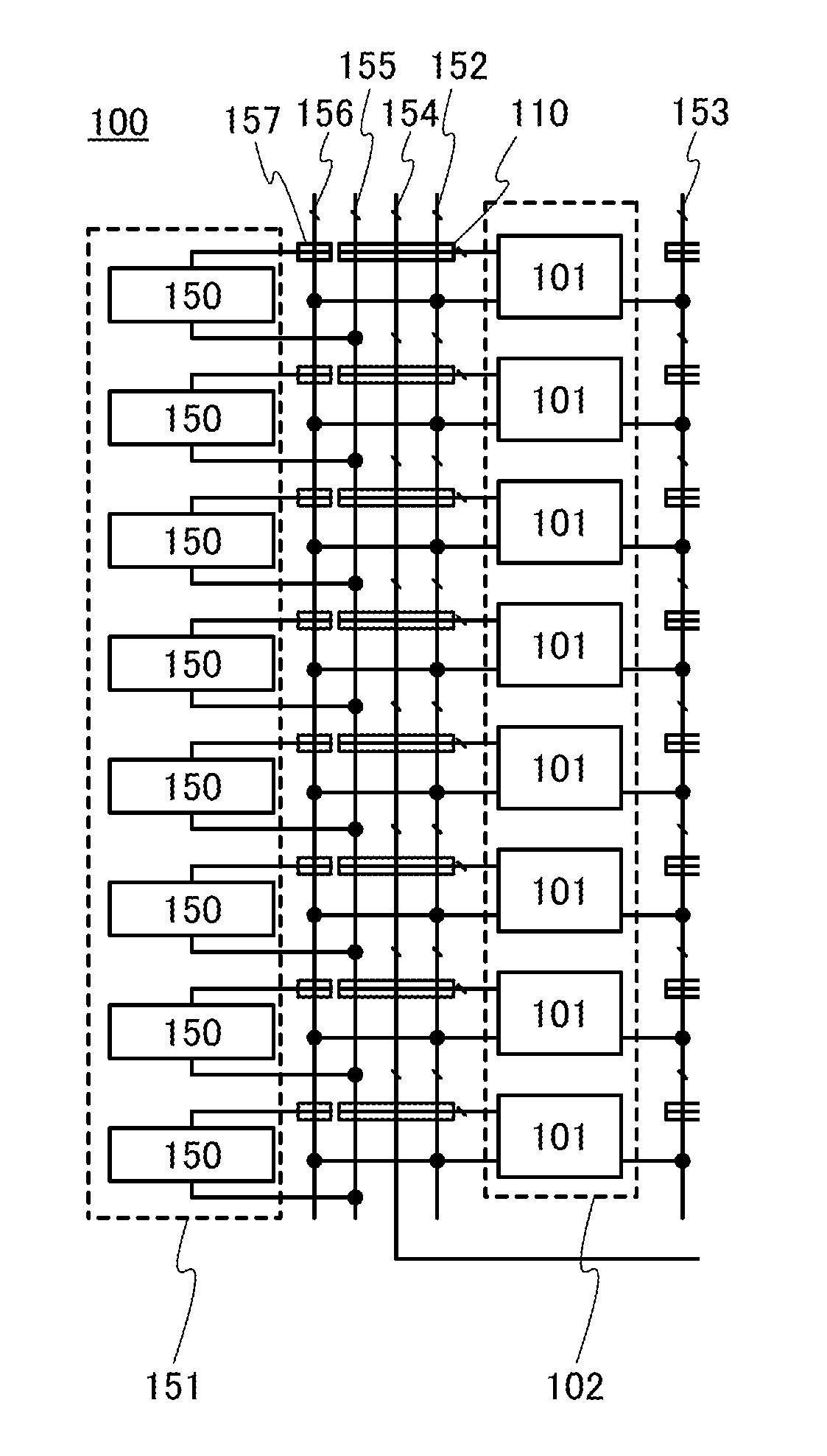
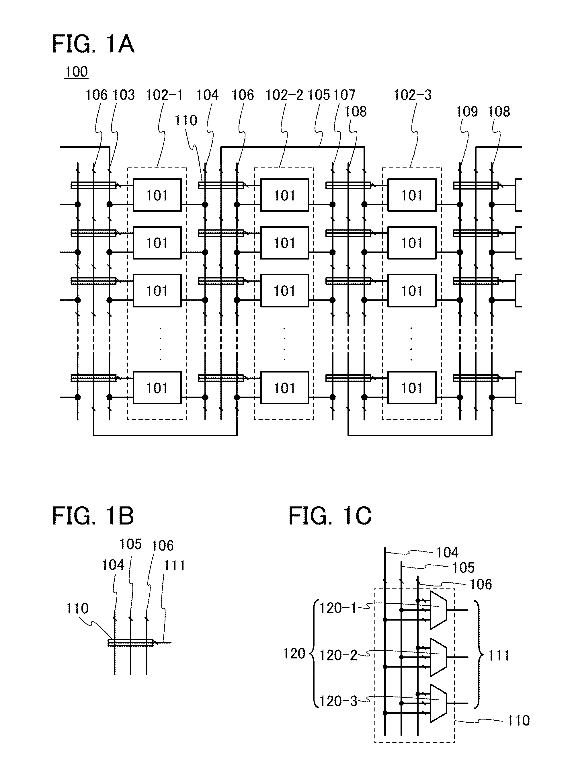
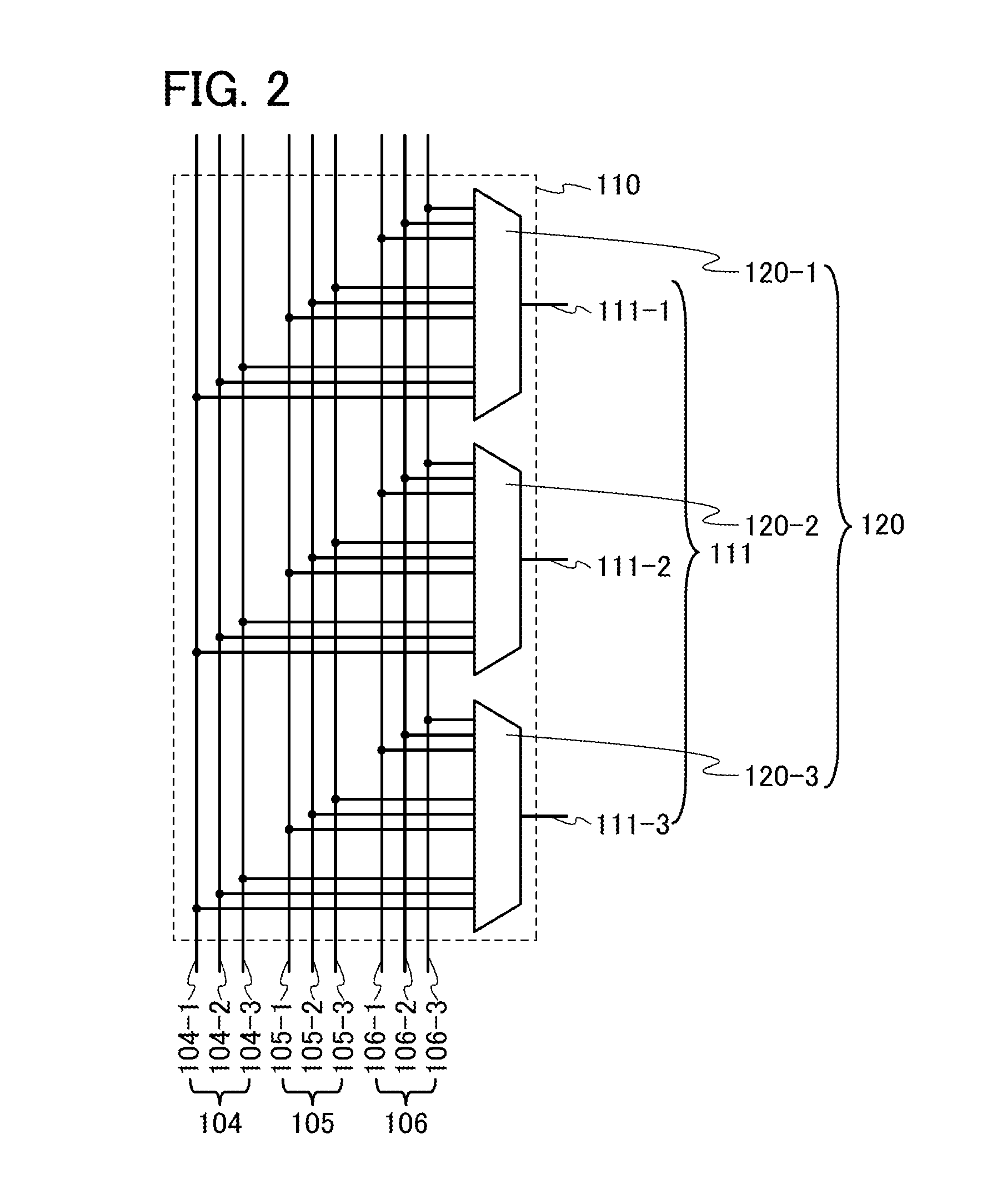
[0073]Embodiments of the present invention will be described below in detail with reference to the accompanying drawings. Note that the present invention is not limited to the following description, and it is easily understood by those skilled in the art that the mode and details can be variously changed without departing from the scope and spirit of the present invention. Accordingly, the present invention should not be construed as being limited to the description of the embodiments below.

[0074]Note that a programmable logic device of the present invention includes, in its category, a variety of semiconductor integrated circuits formed using semiconductor elements, such as microprocessors, image processing circuits, controllers for semiconductor display devices, digital signal processors (DSP), and microcontrollers. A semiconductor device of the present invention includes, in its category, various devices such as RF tags formed using any of the above semiconductor integrated circu...


PUM


Abstract

Provided is a programmable logic device that includes logic elements arranged in a plurality of columns. Wirings connecting logic elements are arranged between the plurality of columns. Switch circuits that control electrical connections between the wirings and the logic elements are also arranged between the plurality of columns. Each of the switch circuit selects an electrical connection between one of the wirings and an input terminal of one of the logic elements in accordance with configuration data.

Description

TECHNICAL FIELD[0001]The present invention relates to an object, a method, or a manufacturing method. The present invention also relates to a process, a machine, a manufacture, or a composition of matter. In particular, the present invention relates to, for example, a semiconductor device, a display device, a light-emitting device, a power storage device, a driving method thereof, or a manufacturing method thereof. One embodiment of the present invention particularly relates to, for example, a programmable logic device in which the configuration of hardware can be changed and a semiconductor device including the programmable logic device.BACKGROUND ART[0002]In a programmable logic device (PLD), a logic circuit is composed of an adequate number of logic elements (basic blocks), and the function of each logic element and interconnections between the logic elements can be changed after manufacture. Specifically, the PLD includes a plurality of logic elements, a routing resource for con...

Claims


Application Information

Patent Timeline
IPC IPC(8): H03K19/177
CPCH03K19/177H03K19/1735H03K19/17728H03K19/1776H03K19/17764H03K19/17792H01L27/1207H01L27/1225H01L27/124H01L29/24H01L29/78648H01L29/7869
Inventor IKEDA, TAKAYUKIKUROKAWA, YOSHIYUKI
Owner SEMICON ENERGY LAB CO LTD
Why Eureka
Try Eureka