
Semiconductor device with flexible redundancy system

Inactive Publication Date: 2005-03-08
KK TOSHIBA
View PDF18 Cites 5 Cited by
  • Summary
  • Abstract
  • Description
  • Claims
  • Application Information

AI Technical Summary

Benefits of technology

This invention has been developed to solve the above-described problems, and has its object to provide a semiconductor device that employs a redundancy circuit of a high saving efficiency and a high area efficiency on a chip, in which the redundancy circuit requires only a small number of non-volatile storage elements to save a defective memory cell.
In the invention, defective cells can be saved in a reliable manner even when they are located at only one area of the memory cell array, by virtue of the structure in which the redundancy cell arrays and mapping information indicative of the relationship between circuits for storing defective cells are stored in the circuits. Moreover, in the invention, the area efficiency of the redundancy circuit can be enhanced by reducing the number of redundancy cell arrays necessary to save defective cells.

Problems solved by technology

On the other hand, the redundancy system requires a spare element and a fuse set in addition to a usual circuit, and hence requires a large chip area.
This type of memory chip cannot have a spare element for saving a defective cell which is included in any other bank.
Although this is mainly a problem of a row spare element, a similar problem will occur with a column spare element.
Moreover, if in memory devices operable at high speed, the distance between a memory cell and another replaced by a spare element becomes longer than before the replacement, transmission delay of a signal or data becomes greater, thereby degrading the high speed operability.
This means that the column spare element cannot cover a wide cell array area.
Moreover, in the conventional system in which one spare element corresponds to one fuse set, the number of fuse sets inevitably increases with an increase in the number of spare elements.
Since, in general, fuses require a larger area than spare elements, the system in which one spare element corresponds to one fuse set results in a large decrease in the area efficiency of the redundancy circuit.

Method used


Image

  • Semiconductor device with flexible redundancy system
  • Semiconductor device with flexible redundancy system
  • Semiconductor device with flexible redundancy system

Examples


Embodiment Construction

The embodiment of the invention will be described with reference to the accompanying drawings.

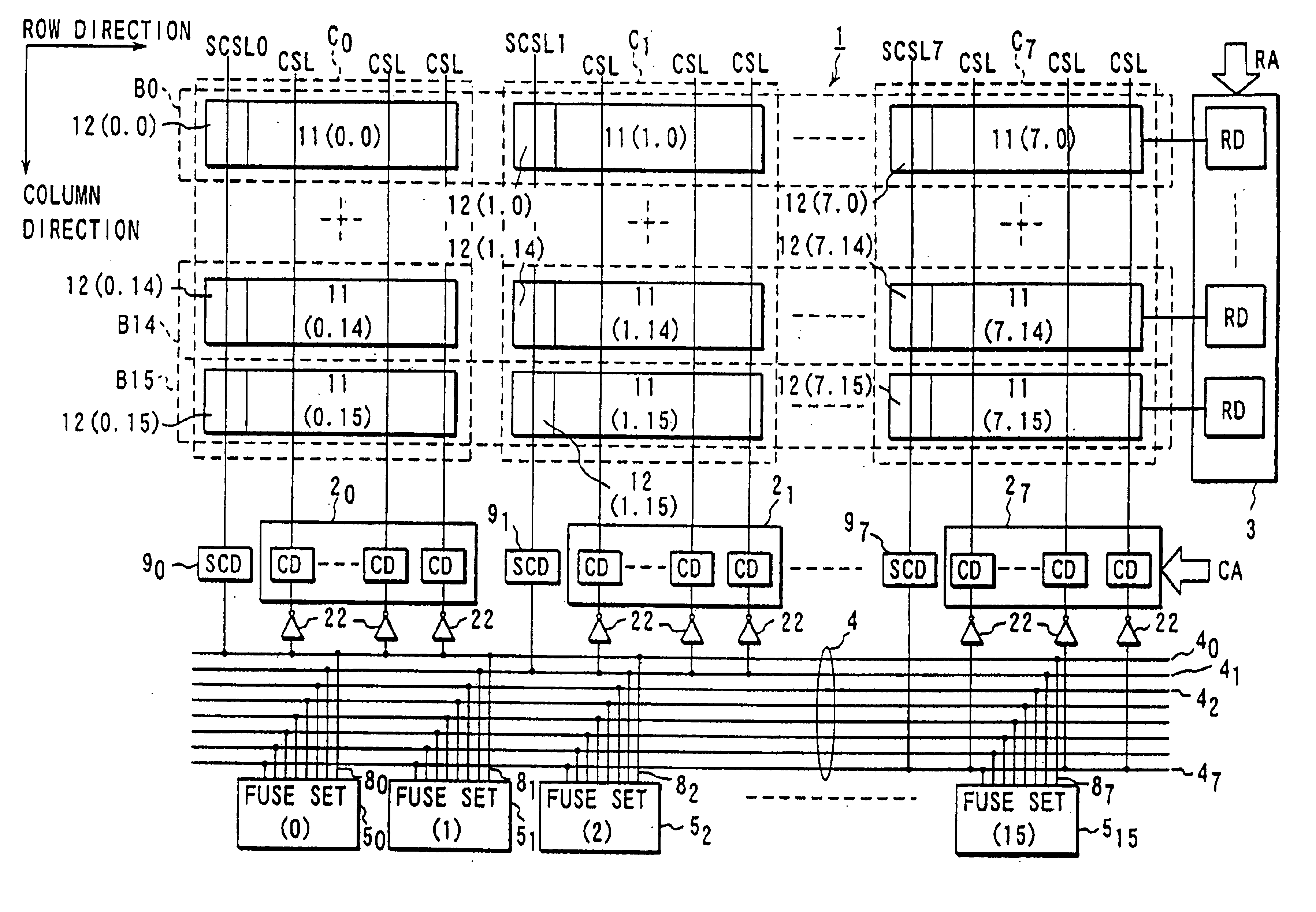
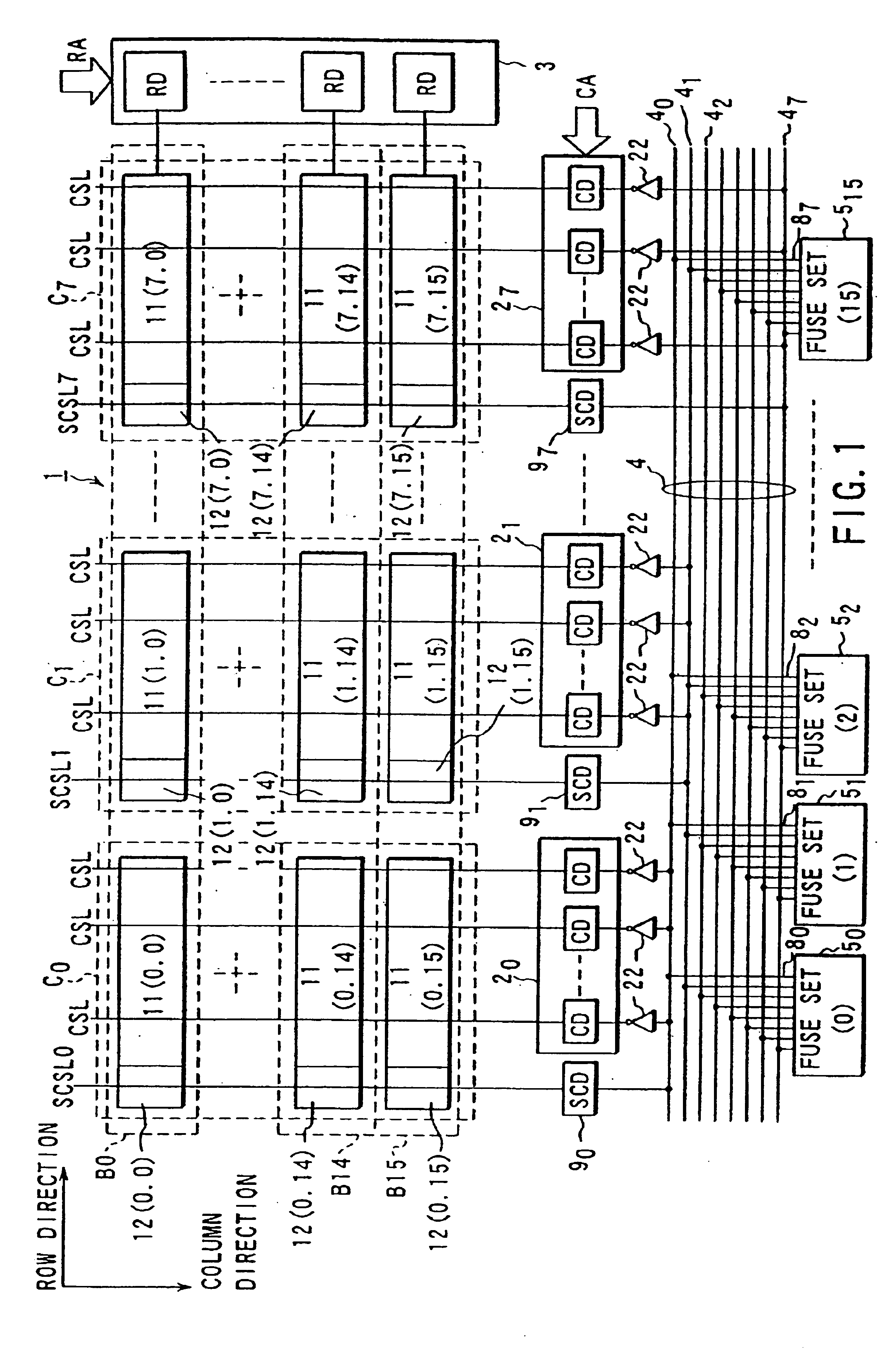
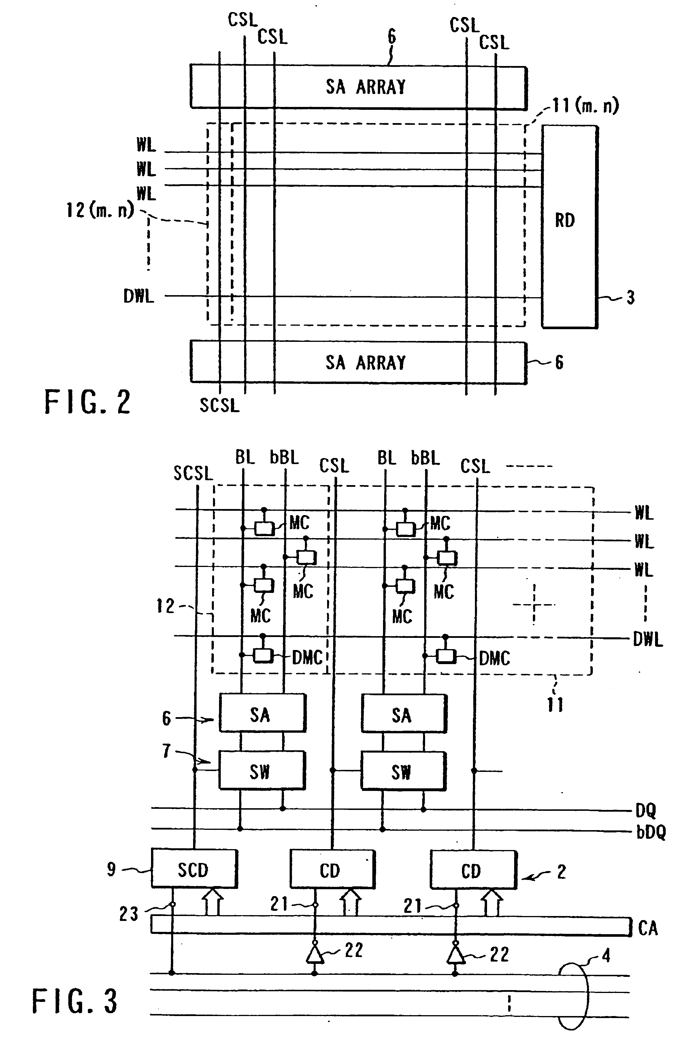
FIG. 1 shows an illustrative structure of a DRAM according to the embodiment of the invention. A memory cell array 1 is divided into sub cell arrays (SCA) 11 (m, n) arranged in a matrix of M (rows)×N (columns). Specifically, the memory cell array 1 is divided into 128 sub cell arrays 11 (m, n) (m: 0-7, n: 0-15) which are obtained by arranging 8 sub cell arrays in each row (M=8) and 16 sub cell arrays in each column (N=16). The division unit of the sub cell arrays 11 is determined on the basis of, for example, the number of columns which can simultaneously transmit data to a data line, and the number of rows (the number of word lines) which are connected to a single sense amplifier array and included in continuous bit lines. In this embodiment, the division unit is also a saving unit in which defective memory cells are saved by a single spare element (redundancy cell array). However, it is p...


PUM


Abstract

A memory cell array includes spare elements for saving a defective cell. Fuse sets each contain a defective address and mapping information indicative of the relationship between the fuse sets and the spare elements. When the defective address matches an input address, each fuse set outputs a signal for activating a corresponding spare element. The number of the fuse sets within a chip is smaller than the number of the spare elements.

Description

BACKGROUND OF THE INVENTIONThis invention relates to a semiconductor device with a flexible redundancy system for saving a defective memory cell.Semiconductor devices have a redundancy system. To enhance the yield of products, the redundancy system saves a defective memory cell, if any, by replacing it with a redundancy cell. The redundancy system that is most generally used at the present stage performs such replacement in units of a cell array, more specifically in units of a plurality of rows or columns (there is a case where it is done in units of one row or column). If in this system, a defective memory cell is found after a test, a cell array including the defective cell is replaced with a redundancy cell array (spare element) of the same size.Address information on a cell array including the defective cell is stored in a non-volatile storage element. A fuse is generally used as the storage element at the present stage. Since the address information is usually formed of severa...

Claims


Application Information

Patent Timeline
IPC IPC(8): G11C7/00G11C29/00
CPCG11C29/812G11C29/808
Inventor TAKASE, SATORU
Owner KK TOSHIBA
Learn More