Circuits configured to remain in a non-program state during a power-down event

a technology of non-program state and power-down event, which is applied in the field of circuits configured to remain in a non-program state during a power-down event, can solve the problems of accidental programming that may be irreversible, corrupt data stored in and unintentionally program the otp memory cell that has not yet been programmed, so as to reduce system cost and complexity

Active Publication Date: 2013-12-03
QUALCOMM INC
View PDF11 Cites 2 Cited by
  • Summary
  • Abstract
  • Description
  • Claims
  • Application Information

AI Technical Summary

Benefits of technology

[0005]Because events at one-time programmable (OTP) memory cells may be irreversible, it is desirable to protect OTP memory cells against ungraceful power-down events. For OTP memories, an ungraceful power-down event may occur when a programming power supply (e.g., a power supply used to set fuses or anti-fuses) stays high while other power supplies fall, which may program or “stress” memory cells of the OTP memory. Conventional techniques may use a separate voltage regulator for the OTP memory array in order to isolate the OTP memory array from other device circuits. However, such a technique results in increased costs associated with multiple voltage regulators as well as increased circuit area. Other techniques may employ switches that are external to the OTP memory array, which may use more area, be more costly to fabricate, and may be less responsive to internal states of the OTP memory array by virtue of being external to the OTP memory array.
[0006]According to at least one embodiment, control circuitry protects OTP memory cells from being accidentally stressed or programmed when an ungraceful power-down event occurs. Further, in at least one embodiment, an OTP memory array is implemented without requiring a separate voltage regulator for the OTP memory cells. Thus, OTP memory cells may share the same voltage regulator with other devices, potentially reducing cost and complexity associated with multiple voltage regulators. According to at least one embodiment, an OTP memory circuit includes multiple internal power switches to decouple OTP memory cells from a programming voltage in response to a power-down event. The OTP memory circuit may include “redundant” protection of the memory cells (e.g., a global power switch in addition to one or more local power switches).
[0010]One particular advantage provided by at least one of the disclosed embodiments is that ungraceful power-down events are less likely to stress or program OTP memory cells of an OTP memory circuit. For example, the OTP memory circuit may be configured to remain in a non-program state during power-down events (e.g., control circuitry may keep the OTP memory array in the non-program state). Further, because the OTP memory circuit is configured to remain in the non-program state during power-down events, a shared voltage regulator may be used to supply both the OTP memory circuit and at least one other device (e.g., a device that accesses data stored in the OTP memory array), which may reduce system cost and complexity associated with use of a separate voltage regulator for the OTP memory circuit.

Problems solved by technology

Because OTP memories may be configured to store information permanently, accidental programming may be irreversible and is therefore generally undesirable.
Accidental programming may occur when an ungraceful power-down event occurs (e.g., an unexpected power failure or an unexpected power-down), which may corrupt data stored in the OTP memory cells (e.g., after such OTP memory cells have been written to) and which may unintentionally program OTP memory cells that have not yet been programmed.
Unintentional programming of OTP memory cells may prevent devices from being updated (e.g., via firmware upgrades to be written to an OTP memory of a wireless communication device), which may be frustrating to users or even dangerous (e.g., where an OTP memory circuit is used in a medical device or in a vehicle).
For OTP memories, an ungraceful power-down event may occur when a programming power supply (e.g., a power supply used to set fuses or anti-fuses) stays high while other power supplies fall, which may program or “stress” memory cells of the OTP memory.
However, such a technique results in increased costs associated with multiple voltage regulators as well as increased circuit area.

Method used


Image

  • Circuits configured to remain in a non-program state during a power-down event
  • Circuits configured to remain in a non-program state during a power-down event
  • Circuits configured to remain in a non-program state during a power-down event

Examples


Embodiment Construction

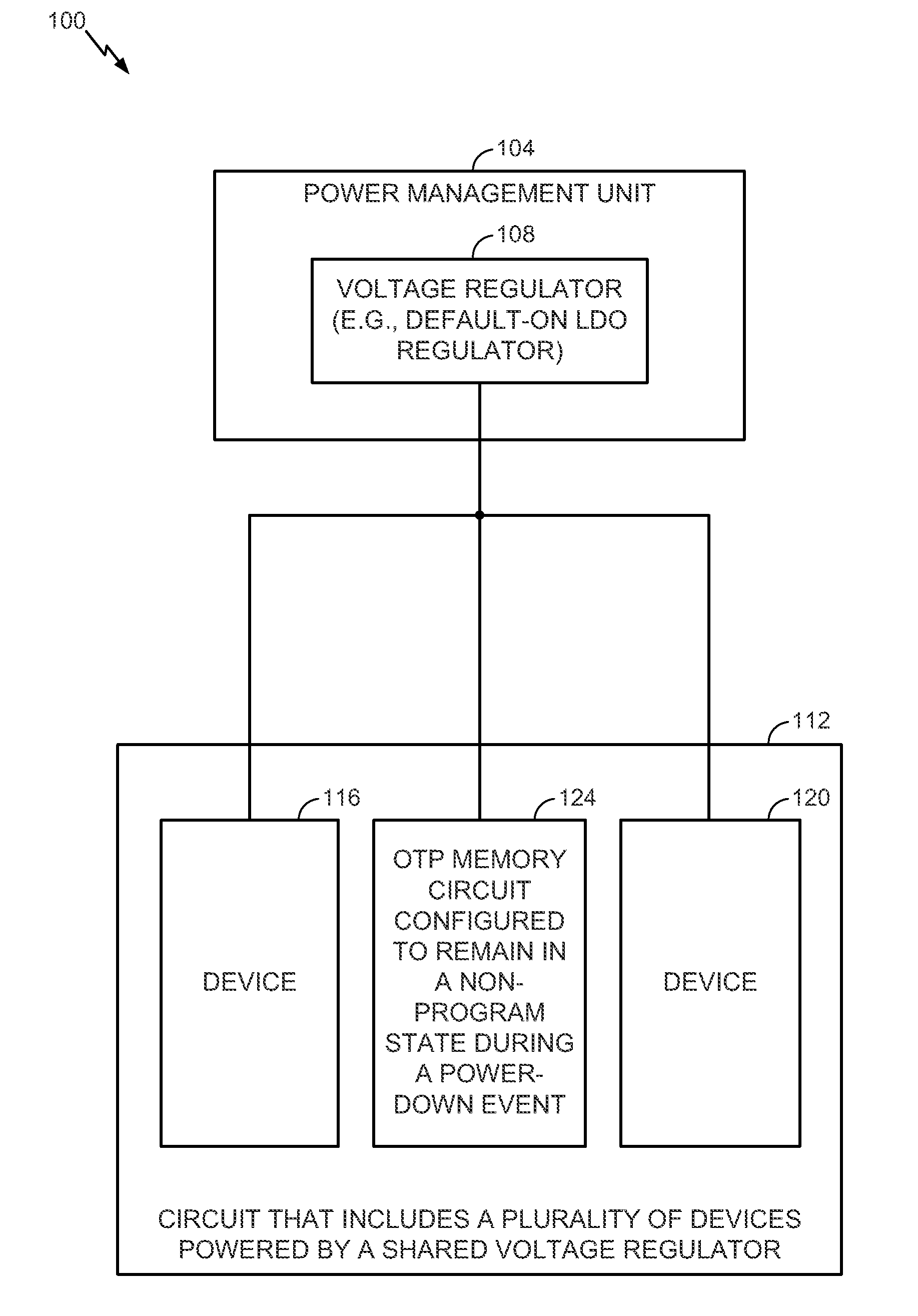
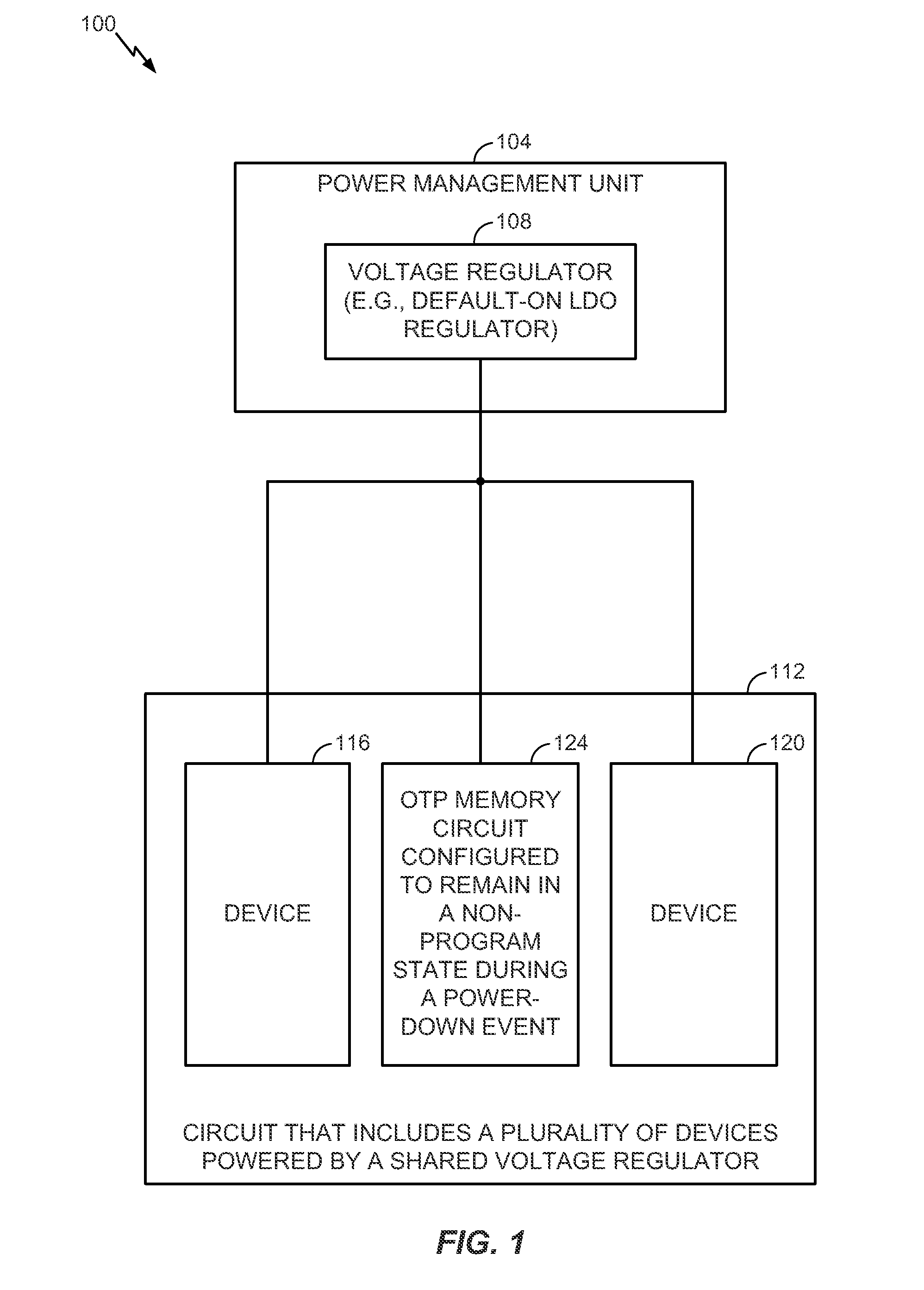
[0018]Referring to FIG. 1, a particular illustrative embodiment of an apparatus is disclosed and generally designated 100. The apparatus 100 may include a power management unit 104 that includes a voltage regulator 108 (e.g., a default-on, low-dropout (LDO) regulator). The apparatus 100 may include a circuit 112 that includes a one-time programmable (OTP) memory circuit 124 and at least one other device. For example, in the embodiment of FIG. 1, the circuit 112 includes a device 116, a device 120, and the OTP memory circuit 112. The OTP memory circuit 112 is configured to remain in a non-program state during a power-down event (e.g., during a power-down event of the circuit 112). The power-down event may be an ungraceful power-down event, such as an accidental or unexpected power-down event.

[0019]As shown in FIG. 1, a plurality of devices (e.g., the device 116, the device 120, and the OTP memory circuit 124) may be configured to share the voltage regulator 108. Utilizing a single vo...


PUM


Abstract

In a particular embodiment, an apparatus includes a one-time programmable (OTP) memory circuit configured to be responsive to a programming voltage. The OTP memory circuit includes an OTP memory array including OTP memory cells, a first power switch configured to decouple the OTP memory array from the programming voltage, and a second power switch configured to decouple a subset of the OTP memory cells from the programming voltage.

Description

I. FIELD[0001]The present disclosure is generally related to circuits configured to remain in a non-program state during a power-down event.II. DESCRIPTION OF RELATED ART[0002]Advances in technology have resulted in smaller and more powerful computing devices. For example, there currently exist a variety of portable personal computing devices, including wireless computing devices, such as portable wireless telephones, personal digital assistants (PDAs), and paging devices that are small, lightweight, and easily carried by users. More specifically, portable wireless telephones, such as cellular telephones and internet protocol (IP) telephones, can communicate voice and data packets over wireless networks. Further, many such wireless telephones include other types of devices that are incorporated therein. For example, a wireless telephone can also include a digital still camera, a digital video camera, a digital recorder, and an audio file player. Also, such wireless telephones can pr...

Claims


Application Information

Patent Timeline
Patent Type & Authority Patents(United States)
IPC IPC(8): G11C17/00G11C5/14
CPCG11C7/24G11C17/18G11C17/16
Inventor TERZIOGLU, ESINUVIEGHARA, GREGORY A.SANI, MEHDI H.KOTA, ANILYOON, SEI SEUNG
Owner QUALCOMM INC
Why Eureka
Try Eureka