Supercharge Your Innovation With Domain-Expert AI Agents!

Semiconductor device

a technology of semiconductor devices and latching devices, applied in the direction of semiconductor devices, electrical equipment, transistors, etc., can solve the problems of semiconductor device destruction, and achieve the effect of suppressing the effect of preventing latching

Active Publication Date: 2013-12-17
DENSO CORP
View PDF9 Cites 2 Cited by
  • Summary
  • Abstract
  • Description
  • Claims
  • Application Information

AI Technical Summary

Benefits of technology

This design effectively mitigates electric field concentration and prevents latchup by allowing for continuous and gradual electric field variation along the trench gate, reducing the impact of manufacturing variations in trench depth.

Problems solved by technology

In a trench gate type semiconductor device, an excessive electric field concentration occurring at a bottom portion of a trench type insulated gate results in destruction of the semiconductor device.

Method used


Image

  • Semiconductor device
  • Semiconductor device
  • Semiconductor device

Examples


first embodiment

[First Embodiment]

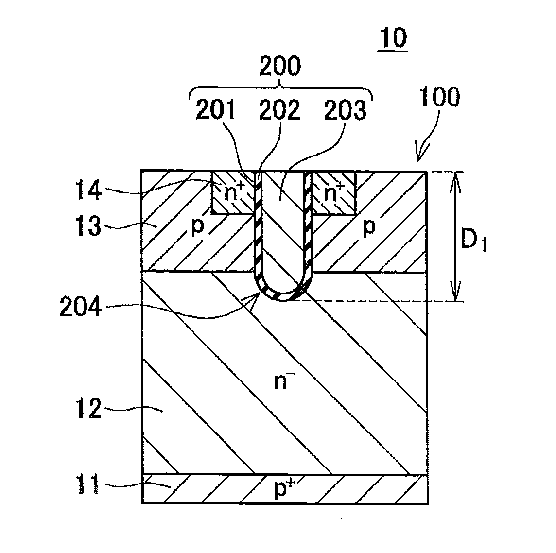
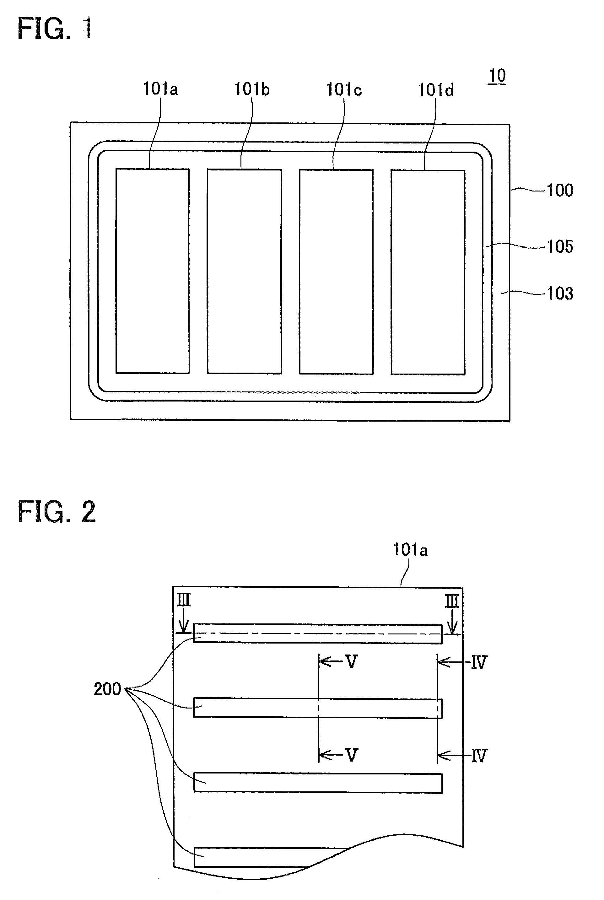
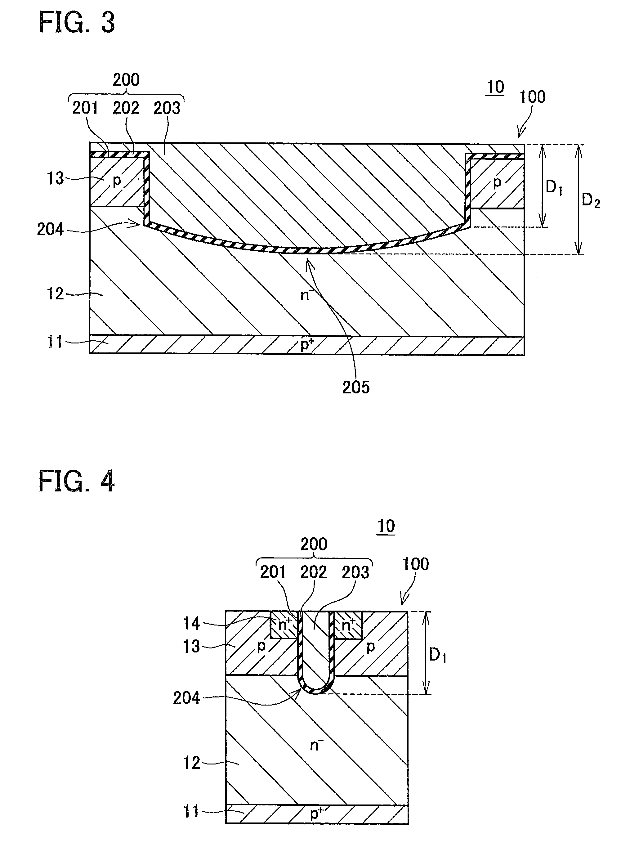
[0070]As shown in FIG. 1, a semiconductor device 10 according to a first embodiment comprises a semiconductor substrate 100 including cell regions 101a to 101d and a non-cell region 103. The cell regions 101a to 101d are arranged at a center portion of the semiconductor substrate 100, and a peripheral termination portion 105 that surrounds the cell regions 101a to 101d is formed in the non-cell region 103. As shown in FIG. 2, a plurality of trench gates 200 is formed in the cell region 101a. The plurality of trench gates 200 is linear in a plan view of the semiconductor device 10, and each of the trench gates 200 has a same size and a same shape. The plurality of trench gates 200 is arranged so that longitudinal directions of the trench gates are parallel to each other. Although not shown, pluralities of trench gates similar to those in the cell region 101a are also formed in the cell regions 101b to 101d.

[0071]As shown in FIGS. 3 to 5, a trench gate type IGBT is ...

second embodiment

[Second Embodiment]

[0084]As shown in FIG. 20, a semiconductor device 40 according to a second embodiment comprises a semiconductor substrate 400 including cell regions 401a to 401d and a non-cell region 403. The cell regions 401a to 401d are arranged at a center portion of the semiconductor substrate 400, and a peripheral termination portion 405 that surrounds the cell regions 401a to 401d is formed in the non-cell region 403. As shown in FIG. 21, a plurality of trench gates 500 is formed in the cell region 401a. All of the trench gates 500 have a same size and a same shape, and are arranged so that longitudinal directions of the trench gates 500 are parallel to each other. Although not shown, pluralities of trench gates similar to those in the cell region 401a are also formed in the cell regions 401b to 401d.

[0085]As shown in FIGS. 22 to 24, a trench gate type IGBT is formed in the cell regions 401a to 401d of the semiconductor device 40. The semiconductor substrate 400 comprises ...


PUM


Abstract

A first semiconductor device comprising: a first conductivity type drift region formed in a semiconductor substrate; a second conductivity type body region formed at an upper surface of the semiconductor substrate on an upper surface side of the drift region; a first conductivity type first semiconductor region formed on a part of an upper surface of the body region; and a trench gate type insulated gate penetrating the first semiconductor region and the body region, and formed to a depth at which the insulated gate contacts the drift region. A part of the insulated gate on a drift region side relative to the body region is deeper at a center portion than at both end portions in a longitudinal direction of the insulated gate.

Description

[0001]This is a 371 national phase application of PCT / JP2011 / 056053 filed 15 Mar. 2011, the contents of which are incorporated herein by reference.TECHNICAL FIELD[0002]The techniques described in the present description relate to a semiconductor device comprising a trench type insulated gate.BACKGROUND ART[0003]In a trench gate type semiconductor device, an excessive electric field concentration occurring at a bottom portion of a trench type insulated gate results in destruction of the semiconductor device. In order to prevent an electric field concentration, for example, Japanese Patent Application Publication No. H9-82954 (Patent Document 1) and Japanese Patent Application Publication No. 2003-174166 (Patent Document 2) describe setting a depth of a trench of an insulated gate at an outermost periphery of an actual operation region shallower than a depth of a trench of another insulated gate in the actual operation region. In addition, Japanese Patent Application Publication No. 2...

Claims


Application Information

Patent Timeline
Patent Type & Authority Patents(United States)
IPC IPC(8): H01L29/80H01L21/28H01L29/76H01L29/78H01L21/336
CPCH01L29/4236H01L29/7813H01L29/7397H01L29/4238
Inventor SENOO, MASARU
Owner DENSO CORP
Features
  • R&D
  • Intellectual Property
  • Life Sciences
  • Materials
  • Tech Scout
  • Unparalleled Data Quality
  • Higher Quality Content
  • 60% Fewer Hallucinations
Learn More