
Embedded DRAM gain memory cell having MOS transistor body provided with a bi-polar transistor charge injecting means

Inactive Publication Date: 2006-04-18
MICRON TECH INC
View PDF63 Cites 210 Cited by
  • Summary
  • Abstract
  • Description
  • Claims
  • Application Information

AI Technical Summary

Benefits of technology

[0017]The above mentioned problems with conventional memories and other problems are addressed by the present invention and will be understood by readi

Problems solved by technology

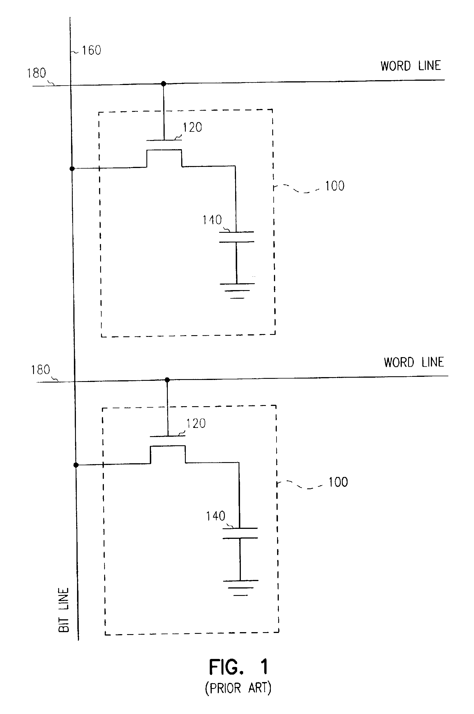
However, reduction in memory cell capacitance reduces the electrical signal output from the memory cells, making detection of the memory cell output signal more difficult.
Thus, as the density of DRAM devices increases, it becomes more and more difficult to obtain reasonable storage capacity.
However, this conflicts with the requirement for larger capacitance because capacitance is proportional to area.
Moreover, the trend for reduction in power supply voltages results in stored charge reduction and leads to degradation of immunity to alpha particle induced soft errors, both of which require that the storage capacitance be even larger.
However, additional masking levels are required in the logic technology to fabricate the trench capacitors.
These type of DRAM cells require only a minor modification of the conventional logic technology processes but occupy a large area due to the use of three transistors.

Method used


Image

  • Embedded DRAM gain memory cell having MOS transistor body provided with a bi-polar transistor charge injecting means
  • Embedded DRAM gain memory cell having MOS transistor body provided with a bi-polar transistor charge injecting means
  • Embedded DRAM gain memory cell having MOS transistor body provided with a bi-polar transistor charge injecting means

Examples


Embodiment Construction

[0028]In the following detailed description of the invention, reference is made to the accompanying drawings which form a part hereof, and in which is shown, by way of illustration, specific embodiments in which the invention may be practiced. The embodiments are intended to describe aspects of the invention in sufficient detail to enable those skilled in the art to practice the invention. Other embodiments may be utilized and changes may be made without departing from the scope of the present invention. In the following description, the terms wafer and substrate are interchangeably used to refer generally to any structure on which integrated circuits are formed, and also to such structures during various stages of integrated circuit fabrication. Both terms include doped and undoped semiconductors, epitaxial layers of a semiconductor on a supporting semiconductor or insulating material, combinations of such layers, as well as other such structures that are known in the art.

[0029]The...


PUM


Abstract

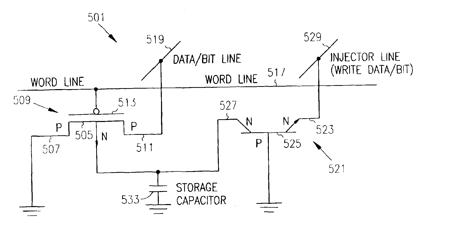
A high density horizontal merged MOS-bipolar gain memory cell is realized for DRAM operation. The gain cell includes a horizontal MOS transistor having a source region, a drain region, and a floating body region therebetween. The gain cell includes a horizontal bi-polar transistor having an emitter region, a base region and a collector region. The collector region for the horizontal bi-polar transistor serves as the floating body region for the horizontal MOS transistor. A gate opposes the floating body region and is separated therefrom by a gate oxide. The emitter region for the horizontal bi-polar transistor is coupled to a write data line.

Description

CROSS REFERENCE TO RELATED APPLICATIONS[0001]This application is related to the following commonly assigned U.S. patent applications: “Single Transistor Vertical Memory Gain Cell,” Ser. No. 10 / 231,397, filed Aug. 29, 2002, “Merged MOS-Bipolar Capacitor Memory Cell,” Ser. No. 10 / 230,929, filed Aug. 29, 2002, each of which disclosure is herein incorporated by reference.FIELD OF THE INVENTION[0002]The present invention relates generally to integrated circuits, and in particular to an embedded DRAM gain memory cell.BACKGROUND OF THE INVENTION[0003]An essential semiconductor device is semiconductor memory, such as a random access memory (RAM) device. A RAM device allows the user to execute both read and write operations on its memory cells. Typical examples of RAM devices include dynamic random access memory (DRAM) and static random access memory (SRAM).[0004]DRAM is a specific category of RAM containing an array of individual memory cells, where each cell includes a capacitor for holdin...

Claims


Application Information

Patent Timeline
IPC IPC(8): H01L27/108H01L27/07H01L29/76H01L29/94
CPCH01L27/0705H01L29/7841H01L27/108H10B12/00
Inventor FORBES, LEONARD
Owner MICRON TECH INC
Learn More