Multi-gate one-transistor dynamic random access memory

a one-transistor, dynamic random access technology, applied in the field of memory devices, can solve the problems of increasing on-current and threshold voltage control, decreasing the dimension of transistor devices, and increasing the difficulty of dealing with short-channel effects

Inactive Publication Date: 2005-03-24
TEXAS INSTR INC
View PDF15 Cites 205 Cited by
  • Summary
  • Abstract
  • Description
  • Claims
  • Application Information

AI Technical Summary

Problems solved by technology

As the dimensions of transistor devices continue to be decreased, however, it is increasingly difficult to deal with short channel effects, increased on-currents and threshold voltage control.
These fringe fields lower the threshold voltage and cause drain induced barrier lowering, which in turn, increases the leakage current of the transistor.
Also, the body is fully depleted so that both gates influence conduction in all parts of the body.
However, with multi-gate transistors that optimally have fully depleted body regions, sufficient storage of charge in the body for the 1T memory is problematic.

Method used


Image

  • Multi-gate one-transistor dynamic random access memory
  • Multi-gate one-transistor dynamic random access memory
  • Multi-gate one-transistor dynamic random access memory

Examples


Embodiment Construction

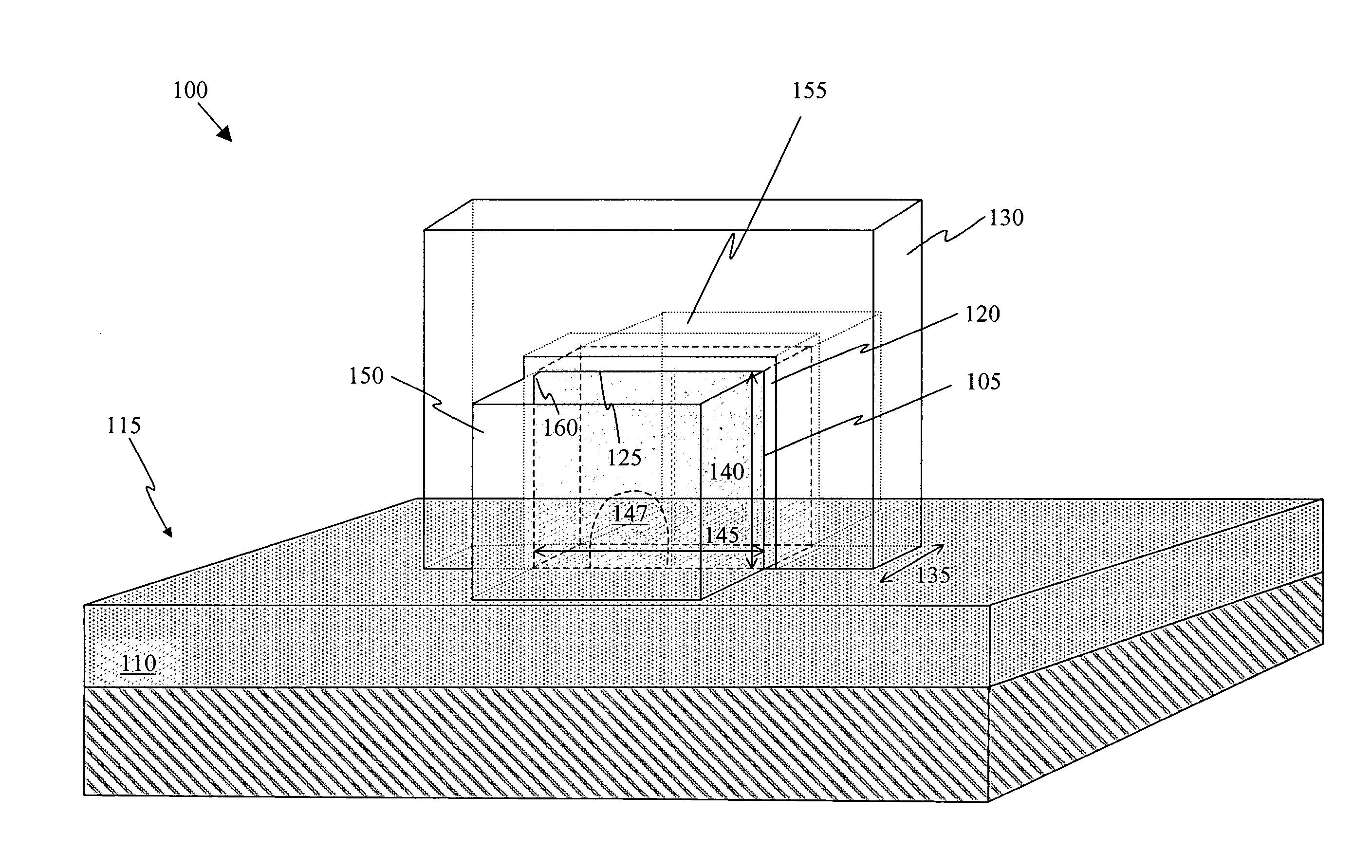
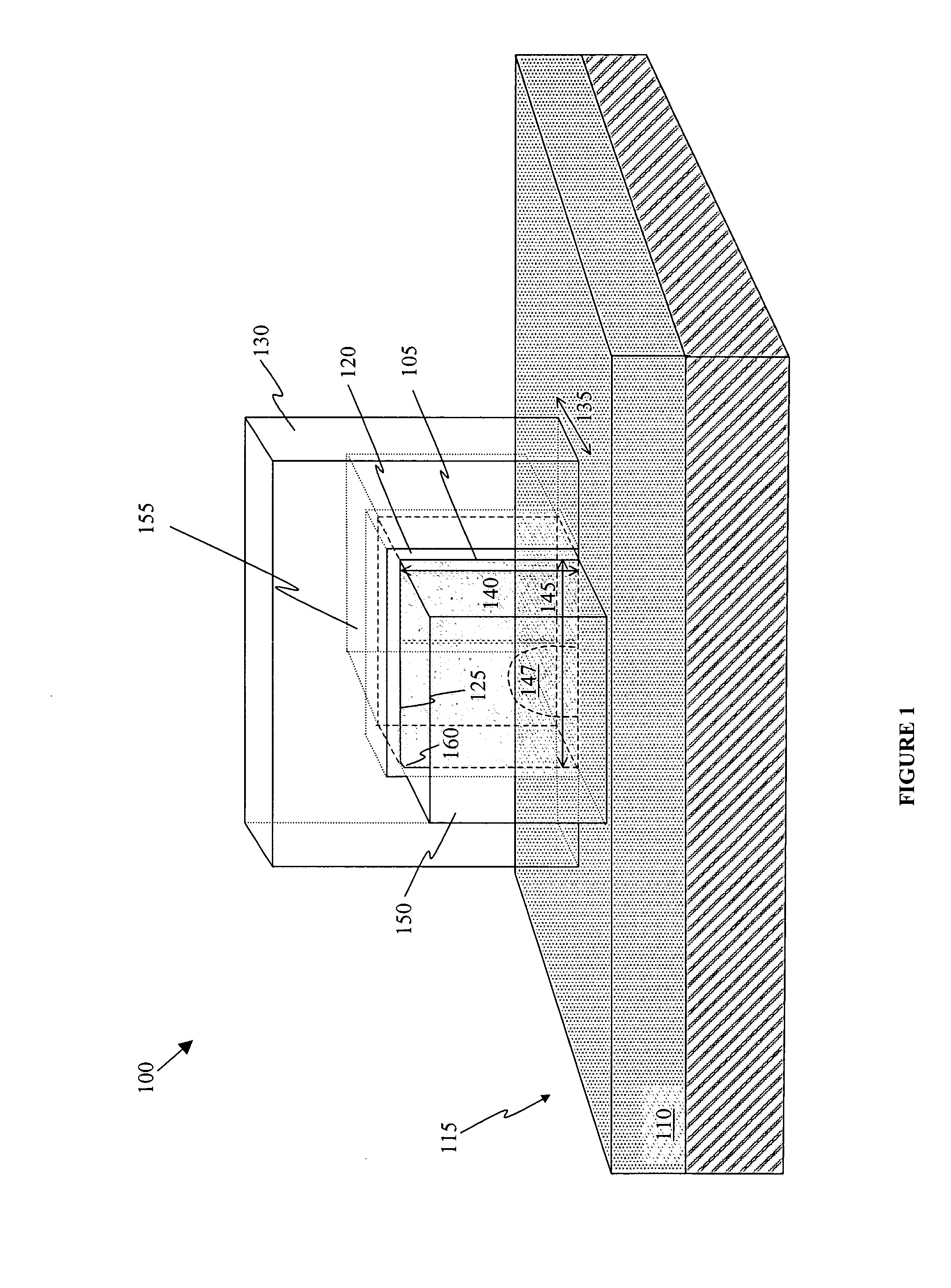
[0015] The present invention recognizes the advantageous use of a multi-gate structure to form a 1T DRAM device. For circuit speed, short gate lengths are desired. Multi-gate transistors offer better control in the channel of the body region, thereby mitigating the above-mentioned deleterious effects of short gate lengths. For instance, multi-gate logic transistors having gate lengths of less about 50 nanometers is highly desirable. It is well known that conventional multi-gate transistors are designed such that the gate workfunction causes the body region to be fully depleted of charge carriers. A fully depleted body region is necessary to get the full benefit of the multi-gate control of the channel. In addition, a fully depleted channel is generally considered to be desirable in logic transistors because this reduces or eliminates floating body effects associated with partially depleted transistors on silicon-on-insulator (SOI) substrates. However, before the present invention, i...


PUM


Abstract

The present invention provides a one-transistor dynamic random access memory (1T DRAM) device (100). The 1T DRAM device (100) includes a body region (105) insulated (110) from a substrate (115) and an insulating layer (120) on a surface of the body region (125). A gate structure (130) is on the insulating layer (120) and conformally surrounding portions of the body region (105). A width of the body region (145) is sufficient to provide a not fully depleted region. Other embodiments include a method of manufacturing a 1T DRAM device (200) and an integrated circuit (300).

Description

TECHNICAL FIELD OF THE INVENTION [0001] The present invention is directed, in general, to memory devices and, more specifically, to a multi-gate one-transistor dynamic random access memory (1T DRAM) device. BACKGROUND OF THE INVENTION [0002] Virtually all microprocessor and digital signal processor applications would benefit from integrated circuits having an increased packing density of memory. A 1T DRAM advantageously eliminates the need for a separate capacitive element associated with a transistor in a conventional DRAM device. To store memory in a 1T DRAM (e.g., logic state “1”), a charge is transiently stored in the body region of a not fully depleted substrate by applying a voltage pulse to the drain. The charge in the body region can be removed (e.g., logic state “0”) by applying an opposite voltage to the drain. The state of charge in the body region changes the threshold voltage (VT) of the 1T DRAM, which in turn, changes the current passing through the channel of the 1T D...

Claims


Application Information

Patent Timeline
Patent Type & Authority Applications(United States)
IPC IPC(8): H01L21/336H01L21/8242H01L21/84H01L27/108H01L27/12H01L29/786
CPCH01L21/845H01L27/108H01L27/10802H01L27/10826H01L29/7854H01L27/1211H01L29/66795H01L29/785H01L27/10897H10B12/20H10B12/36H10B12/00H10B12/50
Inventor HOUSTON, THEODORE W.
Owner TEXAS INSTR INC
Why Eureka
Try Eureka