Bonded semiconductor structure and method of making the same

Inactive Publication Date: 2009-10-29
BESANG
View PDF83 Cites 218 Cited by
  • Summary
  • Abstract
  • Description
  • Claims
  • Application Information

AI Technical Summary

Problems solved by technology

However, these laterally oriented devices consume significant amounts of chip area.
However, forming both horizontal and vertical semiconductor devices on a single major surface of a substrate complicates the processing steps because the masks and processing steps needed are not compatible.
However, a disadvantage of this method is that the laser is capable of driving the temperature of the semiconductor material to be greater than

Method used


Image

  • Bonded semiconductor structure and method of making the same
  • Bonded semiconductor structure and method of making the same
  • Bonded semiconductor structure and method of making the same

Examples


Embodiment Construction

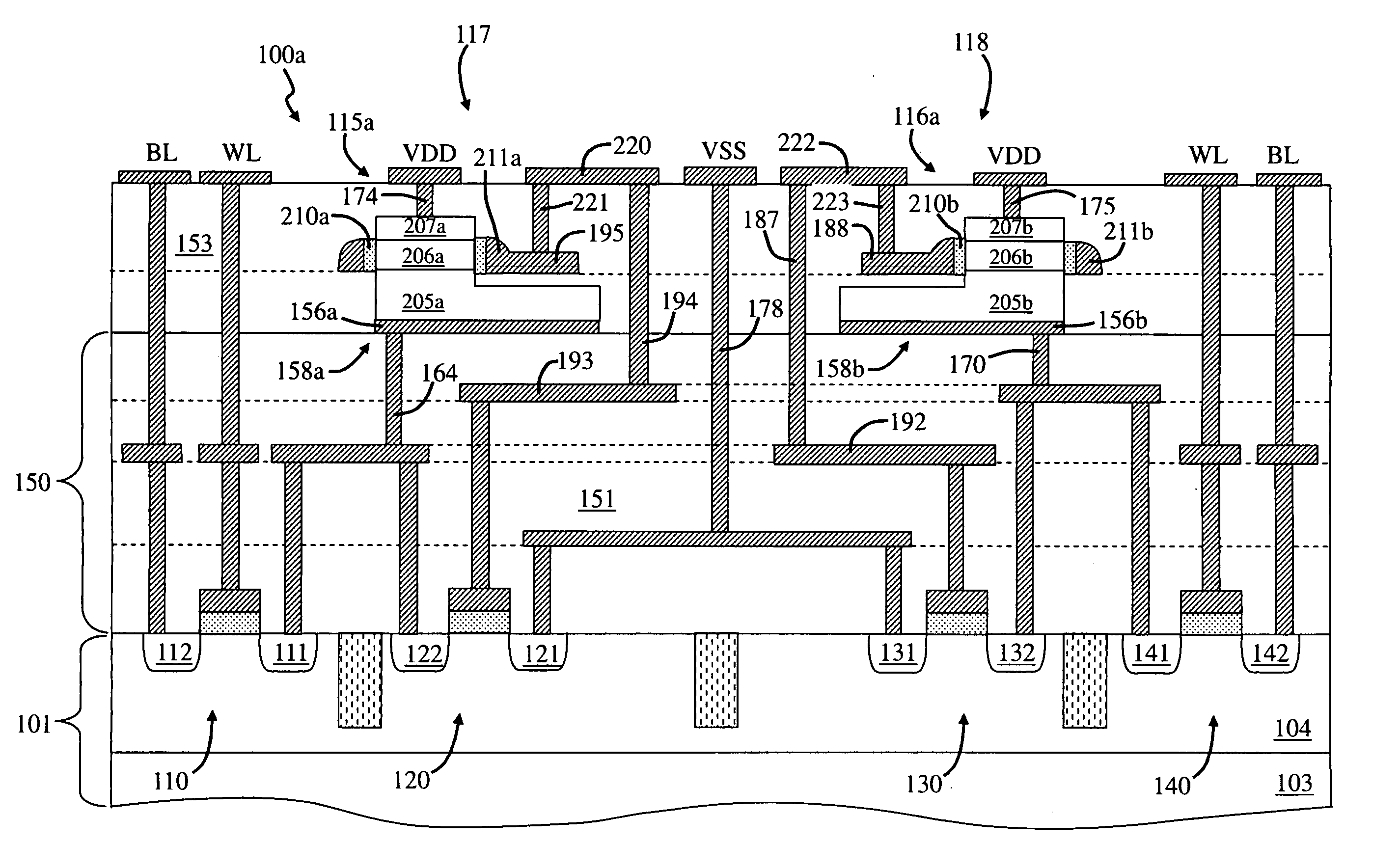
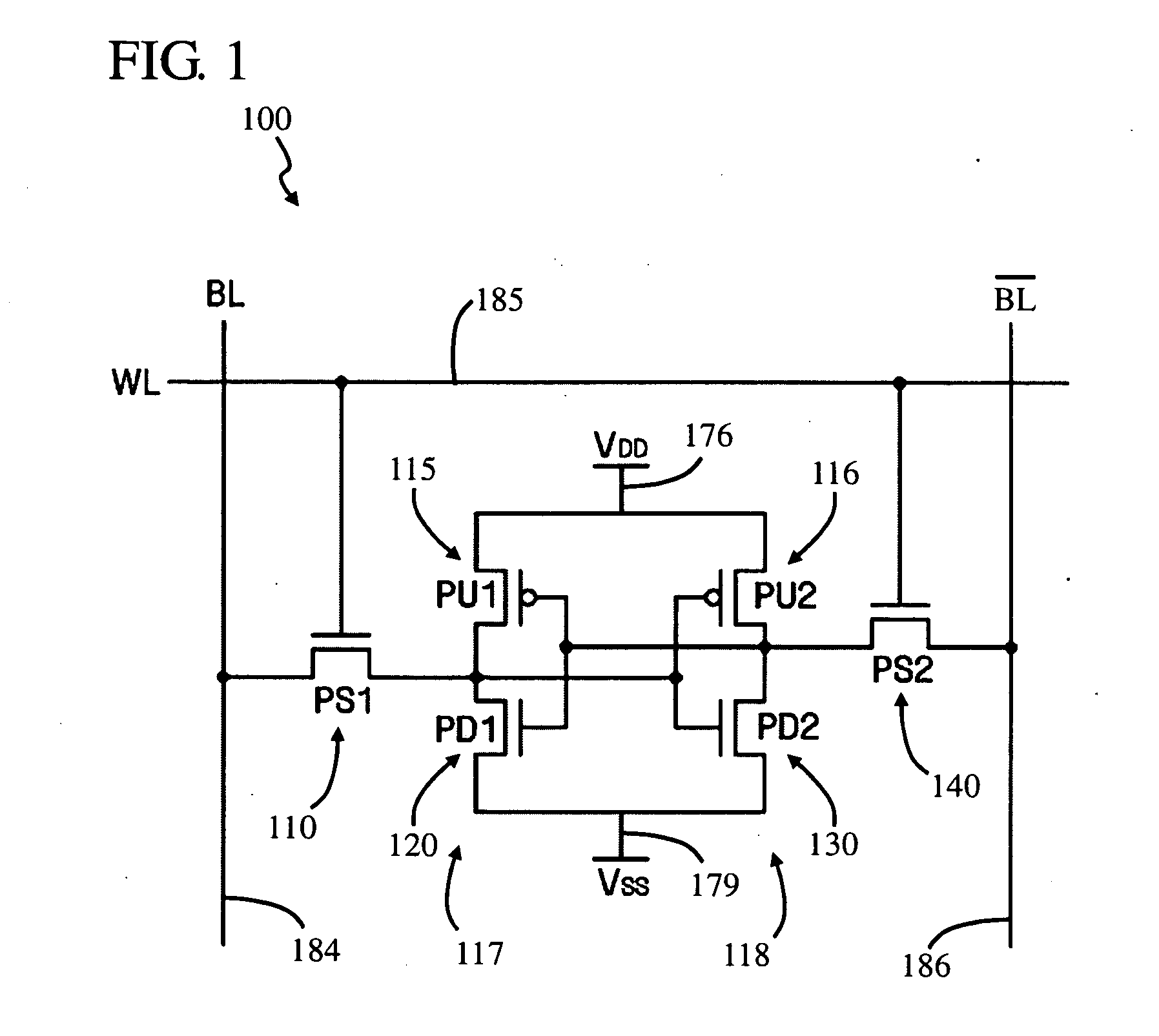
[0029]FIG. 1 is a circuit diagram of a bonded semiconductor structure static random access memory (SRAM) circuit 100. In this embodiment, bonded semiconductor SRAM circuit 100 includes six transistors per SRAM unit cell. However, it should be noted that bonded semiconductor SRAM circuit 100 can include another number of transistors per SRAM unit cell, such as four. It should also be noted that the SRAM unit cell can be repeated a plurality of times to form an array of SRAM unit cells which operate as an SRAM memory array.

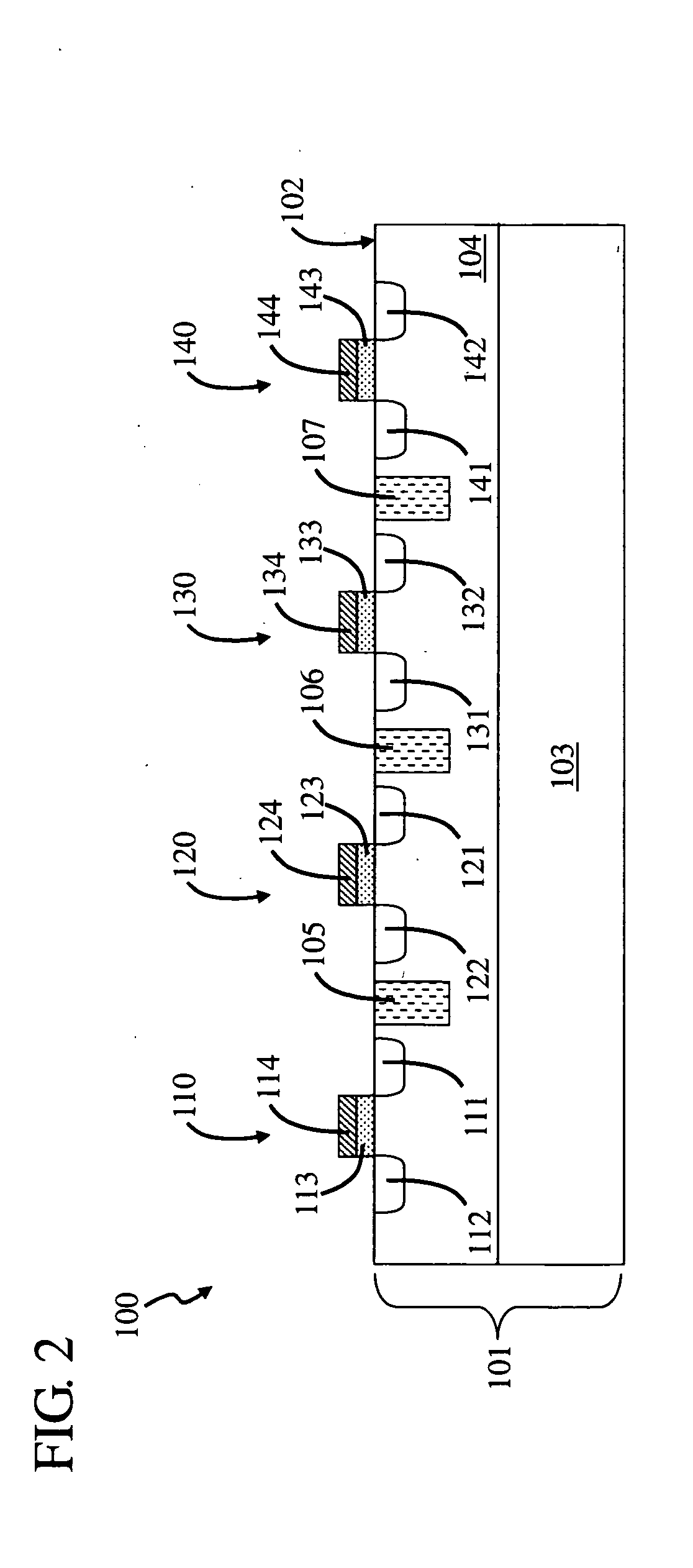
[0030]Bonded semiconductor structure SRAM circuit 100 is a bonded semiconductor structure because, as discussed in more detail below, it includes a bonding region which bonds an electronic device to an interconnect region through a bonding interface. Other semiconductor structures are not bonded semiconductor structures because they do not include a bonding region which bonds an electronic device through a bonding interface.

[0031]In this embodiment, SRAM circuit 100...


PUM


Abstract

A bonded semiconductor structure static random access memory circuit includes a support substrate which carries a first horizontally oriented transistor, and an interconnect region which includes a conductive line. The memory circuit includes a donor substrate which includes a semiconductor layer stack coupled to a donor substrate body region through a detach region, wherein the semiconductor layer stack is coupled to the interconnect region through a bonding interface, and wherein the semiconductor layer stack includes a pn junction.

Description

CROSS-REFERENCE TO RELATED APPLICATIONS[0001]This application claims the benefit of Korean Patent Application No. 10-2008-0046991, filed on May 21, 2008, the contents of which are incorporated herein by reference.[0002]This application is a continuation-in-part of, and claims the benefit of, U.S. patent application Ser. Nos.:[0003]12 / 040,642, filed on Feb. 29, 2008,[0004]11 / 092,498, filed on Mar. 29, 2005, now U.S. Pat. No. 7,470,142,[0005]11 / 092,499, filed on Mar. 29, 2005, now U.S. Pat. No. 7,470,598,[0006]11 / 092,500, filed on Mar. 29, 2005,[0007]11 / 092,501, filed on Mar. 29, 2005;[0008]11 / 092,521, filed on Mar. 29, 2005;[0009]11 / 180,286, filed on Jul. 12, 2005;[0010]11 / 378,059, filed on Mar. 17, 2006; and[0011]11 / 606,523, filed on Nov. 30, 2006;which in turn are continuation-in-parts of, and claim the benefit of, U.S. patent application Ser. No. 10 / 873,969 (now U.S. Pat. No. 7,052,941), filed on Jun. 21, 2004, which claims the benefit of Republic of Korea Patent Application Nos. ...

Claims


Application Information

Patent Timeline
IPC IPC(8): H01L23/48H01L21/30
CPCH01L21/2007H01L21/8221H01L2924/0132H01L2924/01033H01L2924/01023H01L2924/01006H01L24/29H01L2924/19043H01L2924/19042H01L24/83H01L27/0688H01L2224/291H01L2224/8385H01L2924/01013H01L2924/01015H01L2924/01029H01L2924/01032H01L2924/0104H01L2924/01042H01L2924/01049H01L2924/0105H01L2924/01073H01L2924/01074H01L2924/01093H01L2924/04941H01L2924/04953H01L2924/07802H01L2924/13091H01L2924/14H01L2924/19041H01L2924/01014H01L2924/01031H01L2924/3512H01L2924/00H01L2924/12036
Inventor LEE, SANG-YUN
Owner BESANG
Why Eureka
Try Eureka