

Semiconductor device and driving method thereof
a technology of semiconductor devices and driving methods, applied in semiconductor devices, digital storage, instruments, etc., can solve the problems of increased cost per storage capacity, difficulty in reducing power consumption, stored data,
- Summary
- Abstract
- Description
- Claims
- Application Information
AI Technical Summary
Benefits of technology
Problems solved by technology
Method used
Image

Examples
embodiment 1
[Embodiment 1]
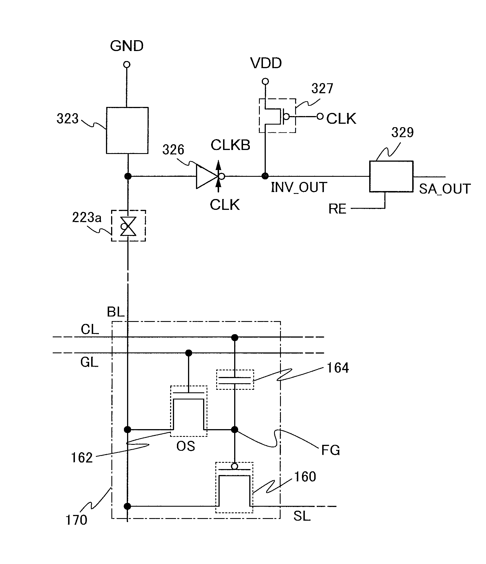
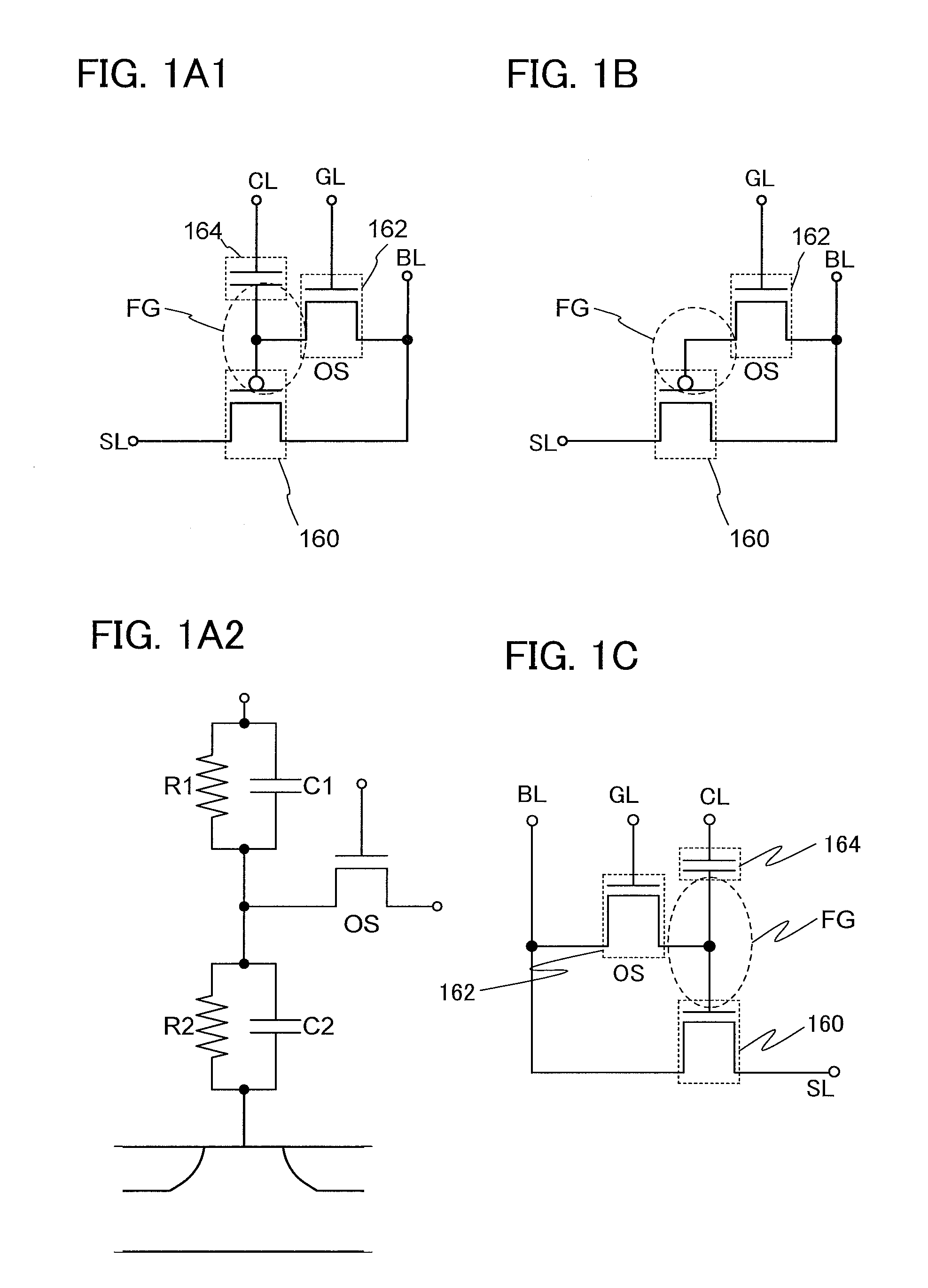
[0079]In this embodiment, a basic circuit configuration and operation of a semiconductor device according to one embodiment of the present invention will be described with reference to FIGS. 1A1, 1A2, 1B, and 1C. Note that in each of circuit diagrams, in some cases, “OS” is written beside a transistor in order to indicate that the transistor includes an oxide semiconductor.
[0080]First, the most basic circuit configuration and its operation will be described with reference to FIGS. 1A1, 1A2, 1B, and 1C. In a semiconductor device illustrated in FIG. 1A1, a bit line BL, a source electrode (or a drain electrode) of a transistor 160, and a source electrode (or a drain electrode) of a transistor 162 are electrically connected to each other. A source line SL is electrically connected to the drain electrode (or the source electrode) of the transistor 160. A gate line GL is electrically connected to a gate electrode of the transistor 162. A gate electrode of the transistor 160 ...
embodiment 2
[Embodiment 2]
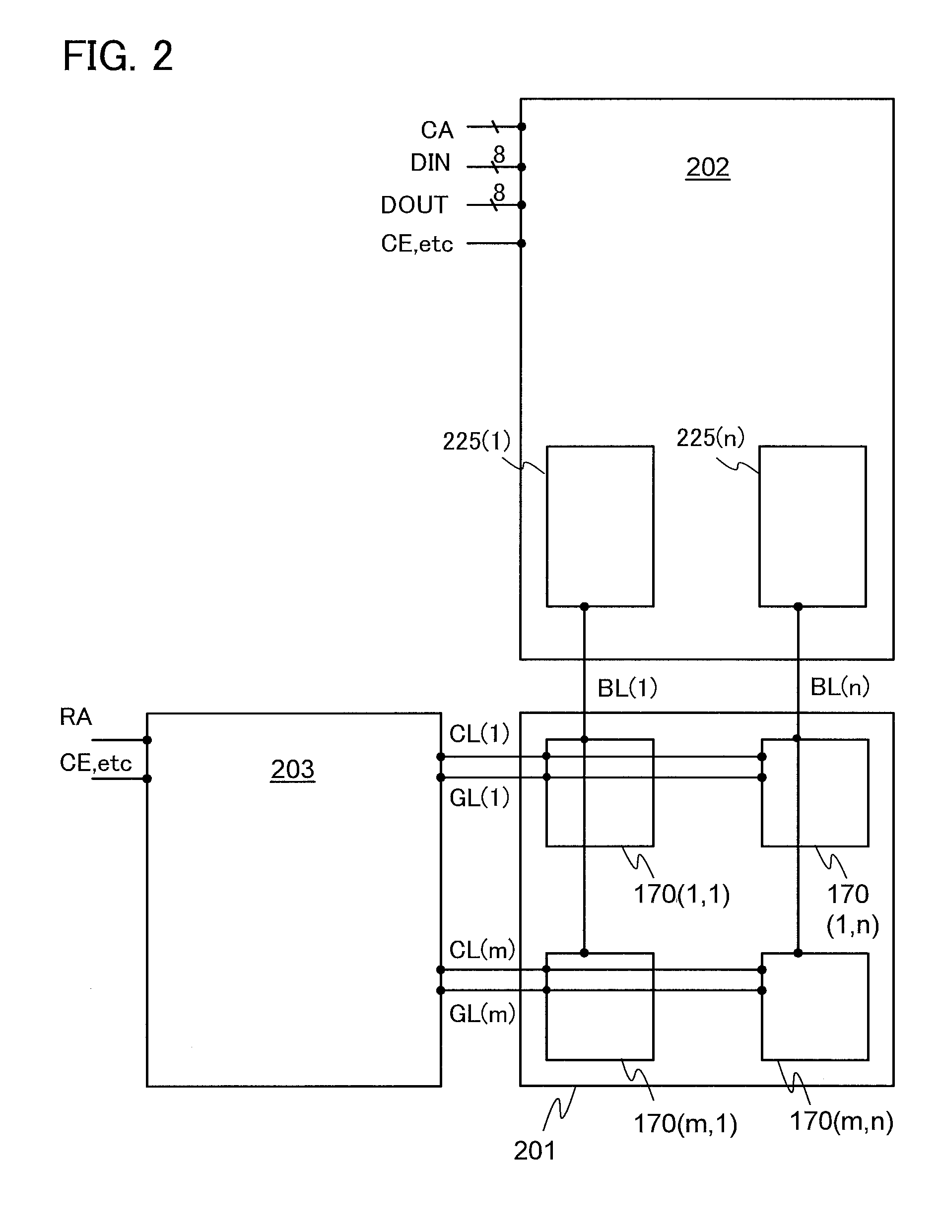
[0210]In this embodiment, a structure of a semiconductor device and a method for manufacturing the semiconductor device according to one embodiment of the present invention will be described with reference to FIGS. 17A and 17B, FIGS. 18A to 18G, FIGS. 19A to 19E, FIGS. 20A to 20D, FIGS. 21A to 21D, and FIGS. 22A to 22C.
[0211]FIGS. 17A and 17B illustrate an example of a structure of a semiconductor device. FIG. 17A illustrates a cross section of the semiconductor device, and FIG. 17B illustrates a plan view of the semiconductor device. Here, FIG. 17A corresponds to the cross section along lines A1-A2 and B1-B2 in FIG. 17B. The semiconductor device illustrated in FIGS. 17A and 17B includes a transistor 160 including a first semiconductor material in a lower portion, and a transistor 162 including a second semiconductor material in an upper portion. Here, the first semiconductor material is preferably different from the second semiconductor material. For example, a semico...
embodiment 3
[Embodiment 3]
[0353]One embodiment of an oxide semiconductor layer which can be used as any of the semiconductor layers of the transistors in the above embodiments will be described with reference to FIGS. 25A to 25C.
[0354]The oxide semiconductor layer of this embodiment has a structure including a first crystalline oxide semiconductor layer and a second crystalline oxide semiconductor layer which is stacked over the first crystalline oxide semiconductor layer and has a larger thickness than the first crystalline oxide semiconductor layer.
[0355]An insulating layer 437 is formed over an insulating layer 400. In this embodiment, an oxide insulating layer with a thickness greater than or equal to 50 nm and less than or equal to 600 nm is formed as the insulating layer 437 by a PCVD method or a sputtering method. For example, a single layer selected from a silicon oxide film, a gallium oxide film, an aluminum oxide film, a silicon oxynitride film, an aluminum oxynitride film, and a sili...
PUM
 Abstract
Description
Claims
Application Information