Semiconductor memory device and method of operation the same

a memory device and semiconductor technology, applied in the field of semiconductor memory devices, can solve the problem of longer time taken to perform copyback operations through external controllers

Inactive Publication Date: 2014-01-07
SK HYNIX INC
View PDF13 Cites 381 Cited by
  • Summary
  • Abstract
  • Description
  • Claims
  • Application Information

AI Technical Summary

Problems solved by technology

Also, the time taken to perform the copyback operation through an external controller is longer than if the method was performed within a chip.

Method used


Image

  • Semiconductor memory device and method of operation the same
  • Semiconductor memory device and method of operation the same
  • Semiconductor memory device and method of operation the same

Examples


Embodiment Construction

[0015]Hereinafter, some exemplary embodiments of the present disclosure will be described in detail with reference to the accompanying drawings. The figures are provided to allow those having ordinary skill in the art to understand the scope of the embodiments of the disclosure.

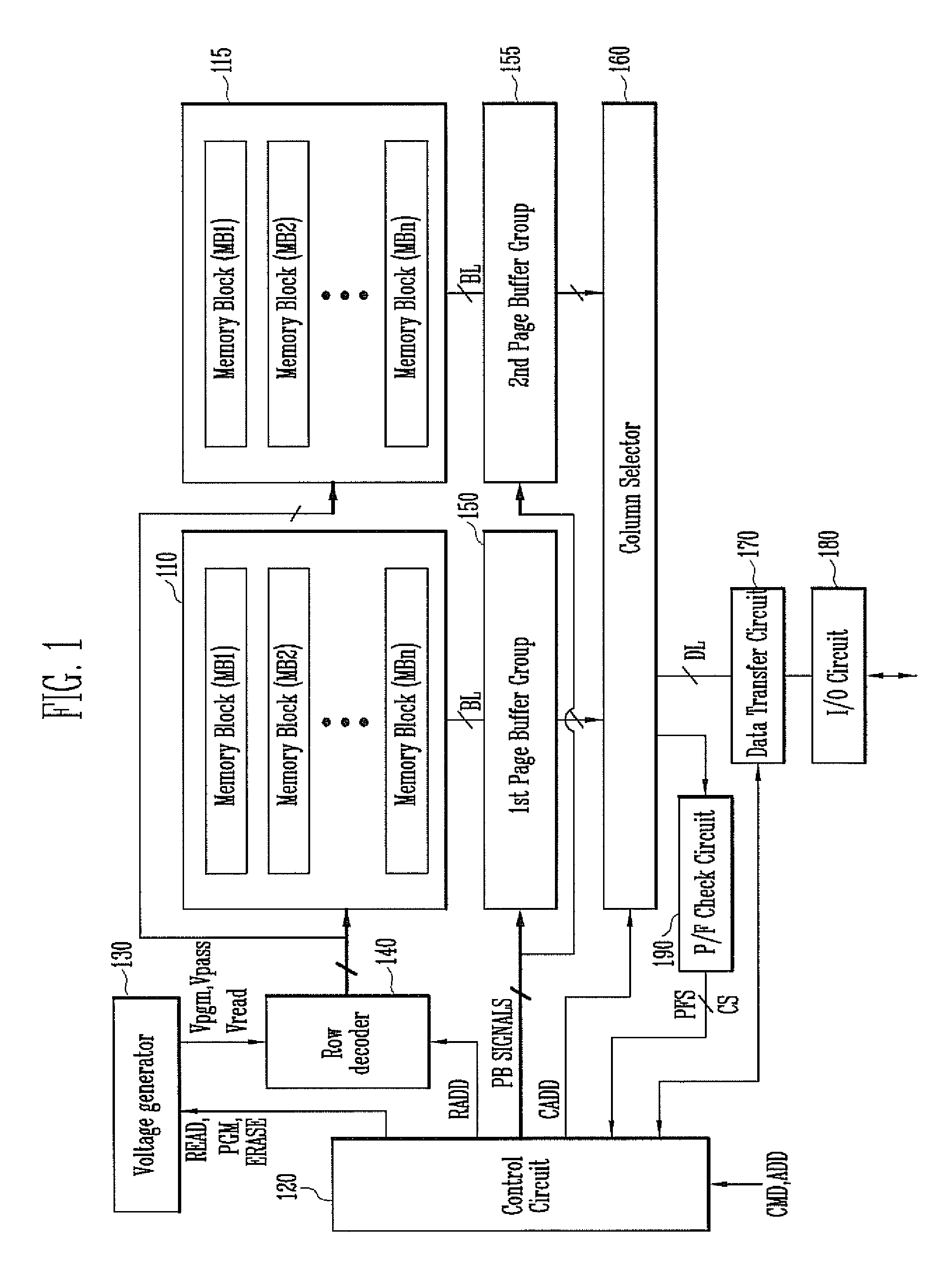
[0016]FIG. 1 is a circuit diagram illustrating the construction of a semiconductor memory device according to an exemplary embodiment of this disclosure.

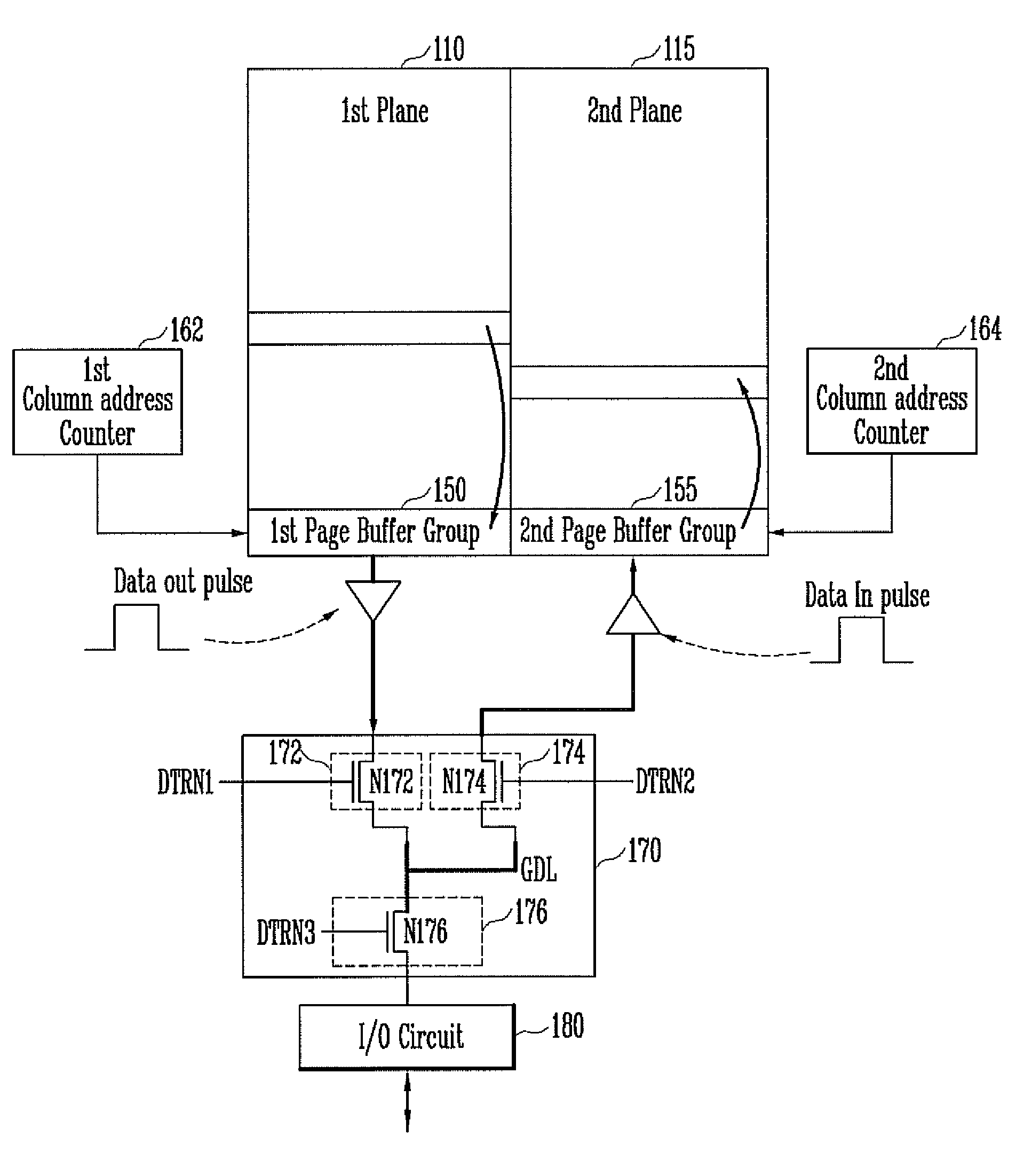
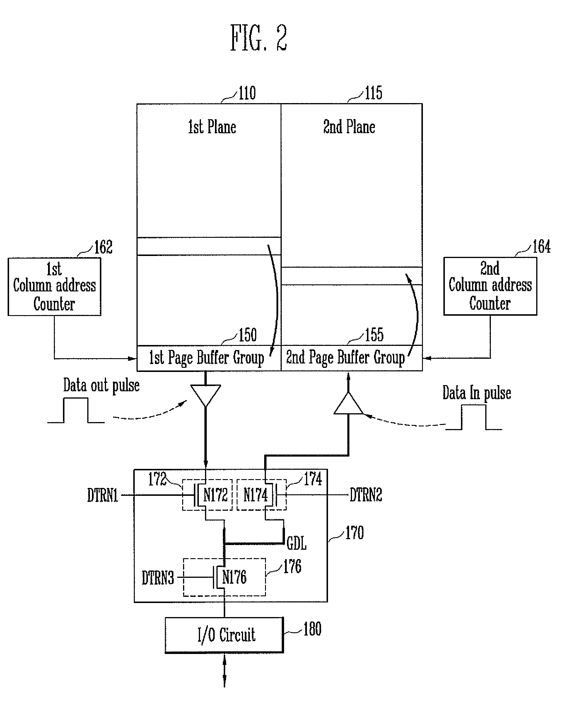
[0017]The semiconductor memory device according to the exemplary embodiment of this disclosure includes first plane and second planes 110 and 115, first and second page buffer groups 150 and 155, and a data transfer circuit 170. A voltage generator 130, a row decoder 140, a column selector 160, an I / O circuit 180, and a pass / fail (P / F) check circuit 190 may be further included as an operation circuit group.

[0018]Each of the first and the second planes 110 and 115 includes a plurality of memory blocks MB1 to MBn.

[0019]Each of the memory blocks includes a plura...


PUM


Abstract

A semiconductor memory device includes a first plane and a second plane each configured to include a plurality of memory cells, and a data transfer circuit configured to transfer first data, stored in the memory cells of the first plane, to the second plane and transfer second data, stored in the memory cells of the second plane, to the first plane when a copyback operation is performed and to transfer the first data or the second data to an I / O circuit when a read operation is performed.

Description

CROSS-REFERENCE TO RELATED APPLICATION[0001]Priority to Korean patent application number 10-2010-0108149 filed on Nov. 2, 2010, the entire disclosure of which is incorporated by reference herein, is claimed.BACKGROUND[0002]Exemplary embodiments relate to a semiconductor memory device and, more particularly, to a semiconductor memory device having a multi-plane structure.[0003]A semiconductor memory device may perform a copyback program operation. The copyback program operation is an operation for reading data of a specific page included in a plane and programming the read data in another page of the specific plane or in another plane. In other words, data of a specific page is copied and stored.[0004]In a conventional semiconductor memory device, data is not transferred between a group of planes forming a memory block when an operation, such as copyback, is performed. Instead, the data must be transferred through an external controller to store the data in another plane. If data is ...

Claims


Application Information

Patent Timeline
Patent Type & Authority Patents(United States)
IPC IPC(8): G11C7/10G11C7/00
CPCG11C7/1006
Inventor JUNG, MIN JOONGLEE, WAN SEOB
Owner SK HYNIX INC
Why Eureka
Try Eureka