Manufacturing method of glass-sealed package, and glass substrate

a manufacturing method and technology of glass shell, applied in the field of manufacturing methods of glass shell and glass shell, can solve the problems of failure to combine the substrate, poor processing accuracy, and low registration accuracy, so as to improve the stability and accuracy of combining the substrate with another substrate, and reduce the amount of warp in the substrate

Inactive Publication Date: 2014-02-25
SEIKO INSTR INC
View PDF23 Cites 0 Cited by
  • Summary
  • Abstract
  • Description
  • Claims
  • Application Information

AI Technical Summary

Benefits of technology

[0009]It is an object of the present invention to reduce an amount of warp in the substrate and to thereby improve the stability and accuracy of combining the substrate with another substrate.
[0010]In order to solve the foregoing problems, the present invention reduces an amount of warp in the substrate by providing a street portion, a region devoid of cavities, extending in a straight line from one end to the other end of the substrate in the form of a frame (a portion where the array pitch is wider than in other portions including the cavities), instead of providing the cavities over the whole surface of the glass substrate portion.
[0011]By the provision of the street portion, the registration accuracy can be stably maintained in the alignment performed in the mating step of combining the substrate with another substrate (such as by anodic bonding). That is, high accuracy and high stability can be realized at the same time.
[0012]As described above, an amount of warp in the glass substrate can be reduced with a manufacturing method of a glass-sealed package of the prevent invention, and with a glass substrate of the present invention. It is therefore possible to realize high registration accuracy and high stability in, for example, the alignment performed in the mating step, thus producing a high-quality glass-sealed package.
[0013]The number of street portions can be optimized according to the size of the substrate so as to minimize a loss in the number of products. In this way, the cost of the product can be minimized.

Problems solved by technology

When the amount of warp in the substrate is excessive, the registration accuracy suffers in the alignment performed in the step of combining the substrate with another substrate (such as by anodic bonding).
In other words, processing accuracy suffers.
This may lead to problems such as a failure to combine the substrates.

Method used


Image

  • Manufacturing method of glass-sealed package, and glass substrate
  • Manufacturing method of glass-sealed package, and glass substrate
  • Manufacturing method of glass-sealed package, and glass substrate

Examples


first embodiment

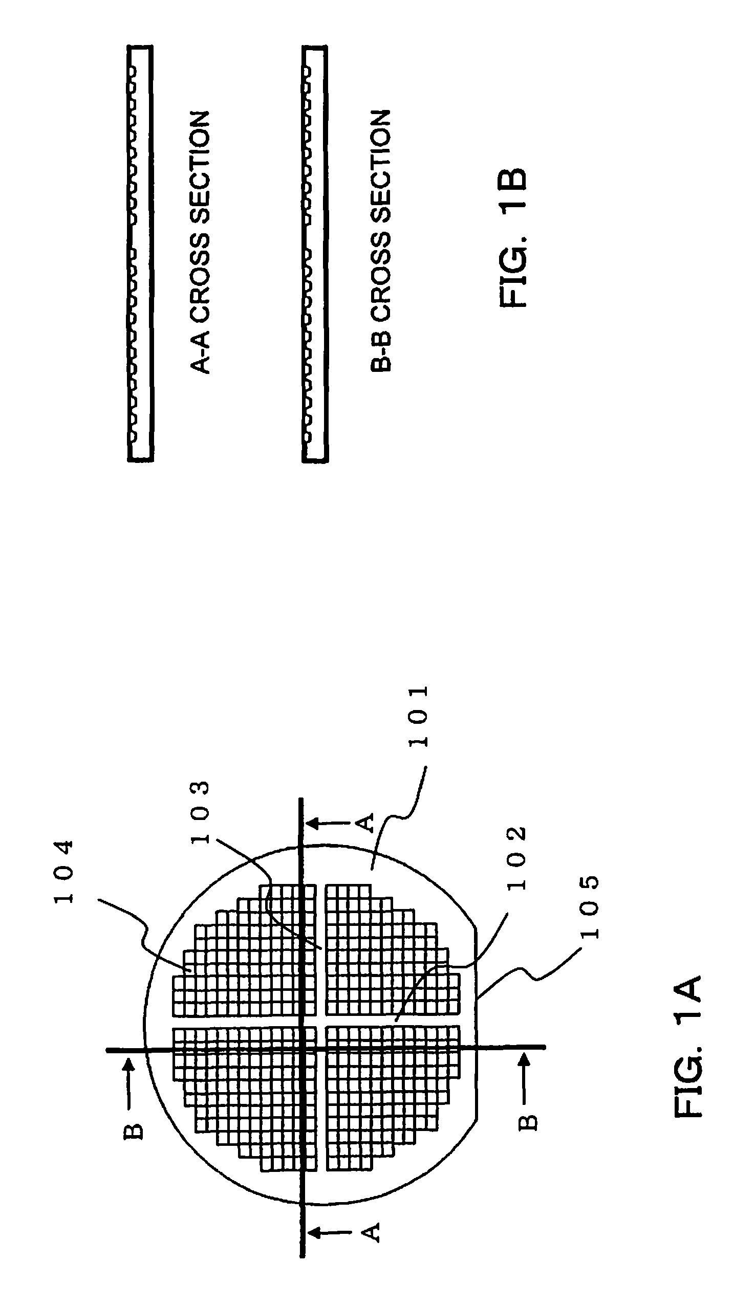
[0020]FIGS. 1A and 1B are diagrams representing a First Embodiment of a glass substrate of the present invention.

[0021]As illustrated in FIG. 1A, a glass substrate of the present invention includes a glass substrate portion 101, cavities 104 in which elements such as semiconductor chips and crystal blanks are housed by being mounted, and an orientation flat 105, which is a cutoff portion formed at one end of the glass substrate portion 101. To reduce warping of the substrate, street portions 102 and 103 are formed in portions of the glass substrate portion 101 where the cavities 104 are formed. The cavities 104 are not formed in the street portions 102 and 103. The street portion 102 is perpendicular to the orientation flat 105, and passes the central portion of the glass substrate portion 101. The street portion 103 is parallel to the orientation flat 105, and passes the central portion of the glass substrate portion 101. The street portions 102 and 103 are formed in a straight lin...

second embodiment

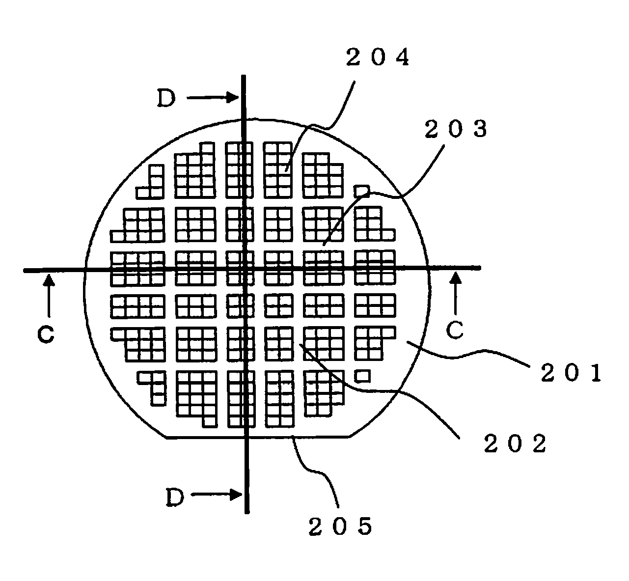
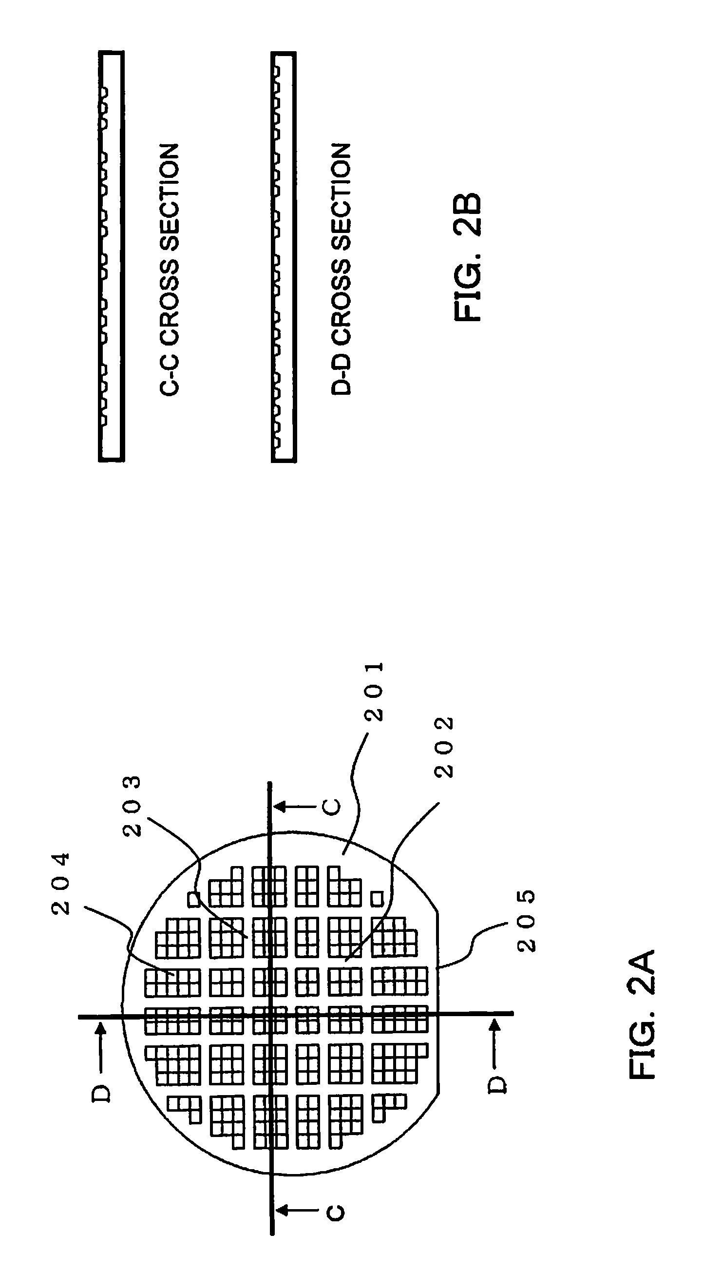
[0042]The Second Embodiment is described below with reference to FIGS. 2A and 2B.

[0043]As illustrated in FIG. 2A, a glass substrate of the present invention includes a glass substrate portion 201, cavities 204 in which elements such as semiconductor chips and crystal blanks are housed by being mounted, and an orientation flat 205, which is a cutoff portion formed at one end of the glass substrate portion 201. To reduce warping of the substrate, street portions 202 and 203 are formed to partially replace the region where the cavities 204 are formed. The cavities 204 are not formed in the street portions 202 and 203. The street portions 202 are provided in a plurality, perpendicular to the orientation flat 205 and separating the cavities 204. The street portions 203 are provided in a plurality, parallel to the orientation flat 205 and separating the cavities 204. The street portions 202 and 203 are formed in a straight line from one end to the other end of the glass substrate portion ...


PUM

PropertyMeasurementUnit
widthaaaaaaaaaa
processing accuracyaaaaaaaaaa
stabilityaaaaaaaaaa

Abstract

The invention provides a manufacturing method of a glass-sealed package, and a glass substrate used for the glass-sealed package, whereby an amount of warp in a glass substrate is reduced to improve processing accuracy in a subsequent step in which the glass substrate is combined (such as by anodic bonding) with another glass substrate provided with a thin film. The front side of the glass substrate includes a region where the cavities used to house electronic devices such as semiconductor IC chips and crystal blanks are not formed. The region devoid of the cavities is provided in the formed of a frame to reduce an amount of warp in the glass substrate.

Description

RELATED APPLICATIONS[0001]This application claims priority under 35 U.S.C. §119 to Japanese Patent Application No. 2009-039334 filed on Feb. 23, 2009, the entire content of which is hereby incorporated by reference.FIELD OF THE INVENTION[0002]The present invention relates to a manufacturing method of a glass-sealed package used for electronic devices such as semiconductor devices and crystal vibrators, and to a glass substrate used for such glass-sealed packages.BACKGROUND ART[0003]A manufacturing method of a glass substrate used for semiconductor devices such as image sensors is known as described in JP-A-2006-282480 and as illustrated in FIG. 5.[0004]This publication describes providing grooves 502 on a glass substrate 501 so that the amount of warp in a thin-film attached glass substrate before being cut into individual pieces by methods such as dicing is reduced to substantially the same level as that in a thin-film attached glass substrate obtained when the glass substrate 501 ...

Claims


Application Information

Patent Timeline
Patent Type & Authority Patents(United States)
IPC IPC(8): C03C27/00
CPCH01L21/50H01L2924/16588H01L23/08H03H3/02H01L2924/14H01L2924/3511H01L2924/0002Y10T428/24479Y10T156/10H01L2924/00
Inventor TANGE, YOSHIHISA
Owner SEIKO INSTR INC
Why Eureka
Try Eureka