Synchronous semiconductor device having delay locked loop for latency control

a semiconductor device and delay lock technology, applied in the field of semiconductor design technology, can solve problems such as delay corresponding

Active Publication Date: 2014-03-18
SK HYNIX INC
View PDF25 Cites 5 Cited by
  • Summary
  • Abstract
  • Description
  • Claims
  • Application Information

AI Technical Summary

Benefits of technology

[0022]A delay time additionally generated on an internal command path with respect to a clock path is compensated, so that a margin between a delay locked clock and an internal command may be secured, especially in a high frequency environment, where this effect may be significant.

Problems solved by technology

However, the delayed internal command CMDD causes delay corresponding to the fifth delay time tD5 as compared with the delay locked clock DLLCLK.

Method used


Image

  • Synchronous semiconductor device having delay locked loop for latency control
  • Synchronous semiconductor device having delay locked loop for latency control
  • Synchronous semiconductor device having delay locked loop for latency control

Examples


Embodiment Construction

[0031]Exemplary embodiments of the present invention will be described below in more detail with reference to the accompanying drawings. The present invention may, however, be embodied in different forms and should not be construed as limited to the embodiments set forth herein. Rather, these embodiments are provided so that this disclosure will be thorough and complete, and will fully convey the scope of the present invention to those skilled in the art. Throughout the disclosure, like reference numerals refer to like parts throughout the various figures and embodiments of the present invention. In this specification a singular form may include a plural form as long as it is not specifically mentioned in a sentence.

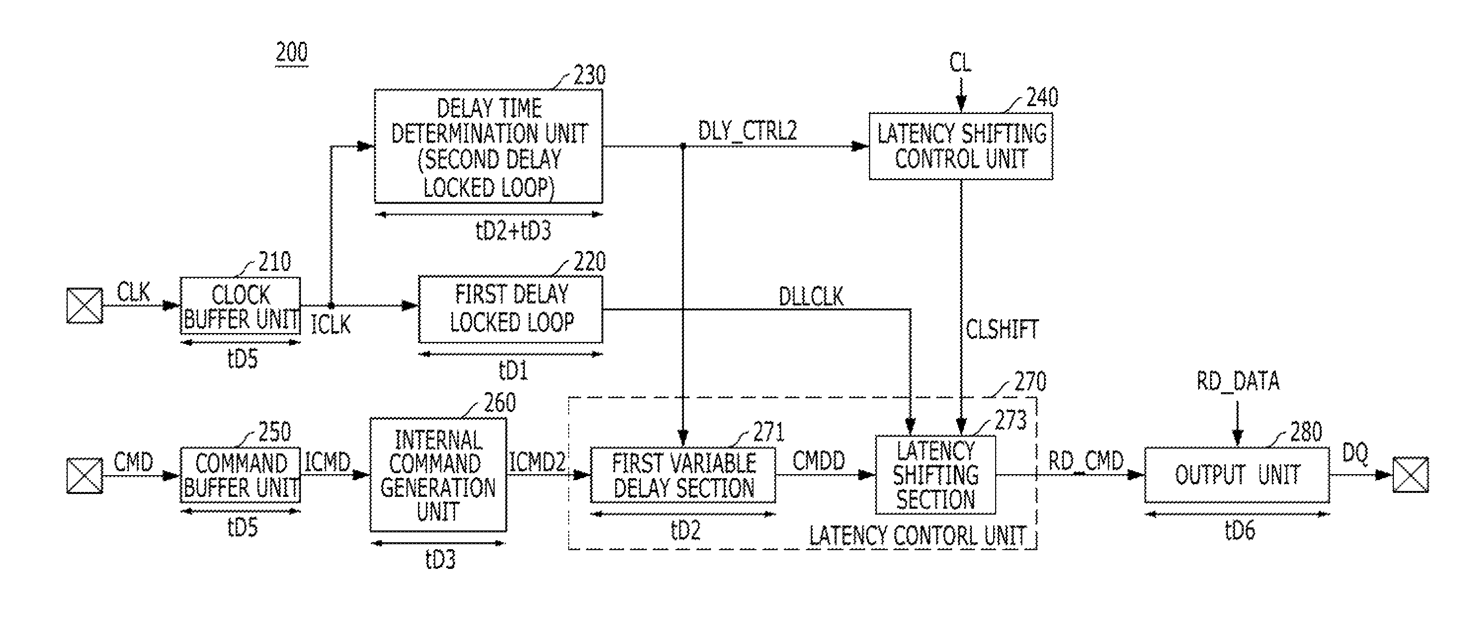
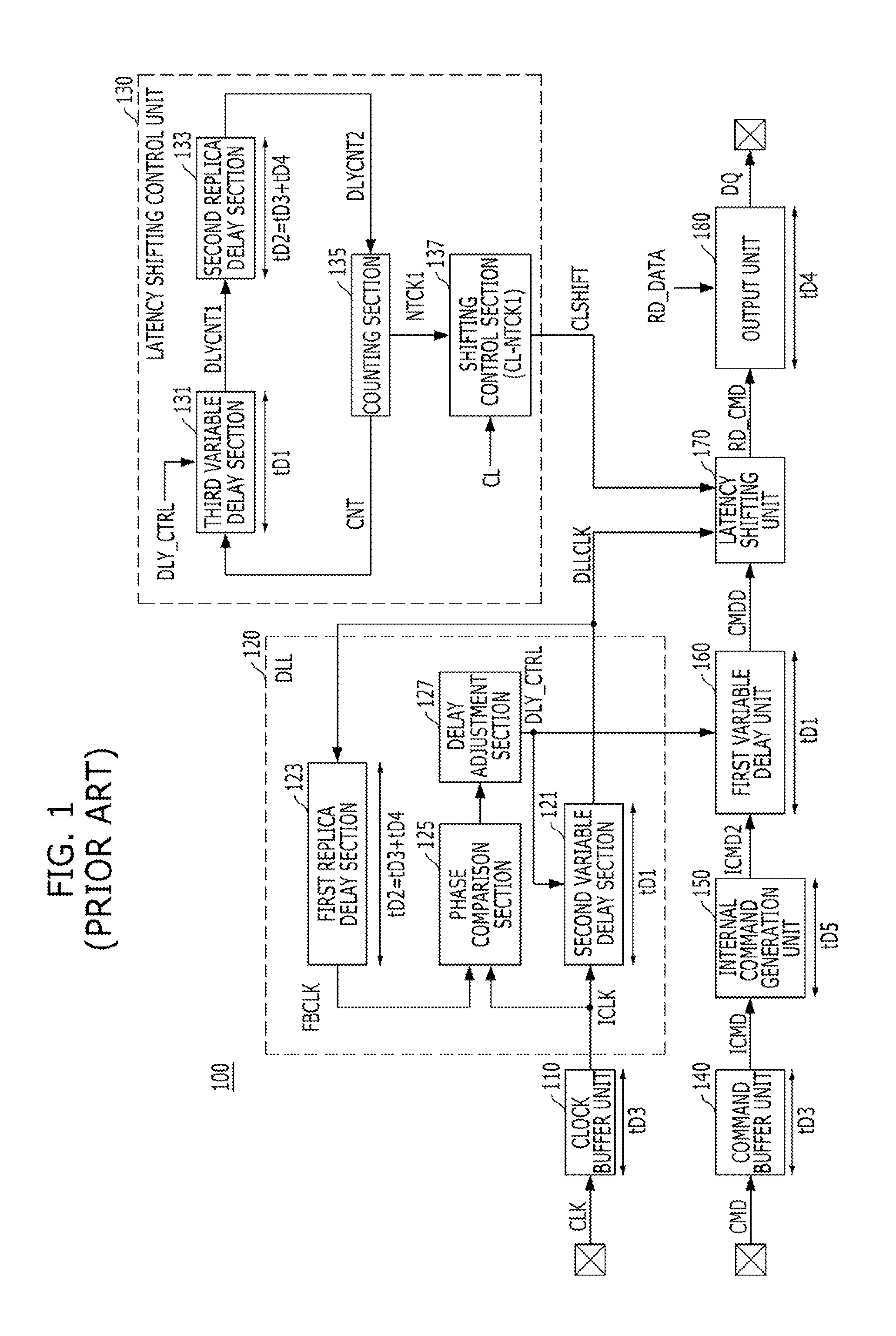
[0032]FIG. 3 is a block diagram illustrating a synchronous semiconductor device in accordance with an embodiment of the present invention, FIG. 4 is a detailed diagram of a first delay locked loop shown in FIG. 3, FIG. 5 is a detailed diagram of a delay time determinatio...


PUM


Abstract

A synchronous semiconductor device includes an internal command generation unit configured to generate an internal command corresponding to a source command, a delay locked loop configured to delay a source clock by a first delay time required for delay-locking to generate a delay locked clock, a delay time determination unit configured to determine a second delay time for delay-locking the internal command using the source clock, the second delay time being determined by reflecting a third delay time generated on a command path, and a latency control unit configured to shift the internal command by a shifting period, in which the second delay time is reflected, in response to the delay locked clock.

Description

CROSS-REFERENCE TO RELATED APPLICATION[0001]The present application claims priority of Korean Patent Application No, 10-2012-0077187, filed on Jul. 16, 2012, which is incorporated herein by reference in its entirety.BACKGROUND[0002]1. Field[0003]Exemplary embodiments of the present invention relate to a semiconductor design technology, and more particularly, to a synchronous semiconductor device having a delay locked loop (DLL) for latency control.[0004]2. Description of the Related Art[0005]In general, a synchronous semiconductor device, such as a double data rate synchronous dynamic random access memory DDR SDRAM), outputs data according to a delay locked loop (DLL) and column address strobe (CAS) latency in a read operation. The CAS latency indicates the number of clock cycles until first data is output through a data pad from a read command synchronized with an external clock.[0006]FIG. 1 is a block diagram illustrating a conventional synchronous semiconductor device.[0007]Refer...

Claims


Application Information

Patent Timeline
Patent Type & Authority Patents(United States)
IPC IPC(8): H03L7/06
CPCH03L7/0816H03L7/081G11C7/1066G11C7/00G11C7/222H03L7/07G11C8/00G11C7/22
Inventor JUNG, JONG-HO
Owner SK HYNIX INC
Why Eureka
Try Eureka