Premetal dielectric integration process

a technology of dielectric integration and dielectric plate, which is applied in the direction of basic electric elements, electrical equipment, semiconductor/solid-state device manufacturing, etc., can solve the problems of reducing budgets, increasing the difficulty of high aspect ratio (ar) features, and void-free filling of narrow widths

Active Publication Date: 2014-04-01
NOVELLUS SYSTEMS
View PDF115 Cites 62 Cited by
  • Summary
  • Abstract
  • Description
  • Claims
  • Application Information

AI Technical Summary

Benefits of technology

[0009]Another aspect relates to a method for filling a gap including providing a workpiece including a gap; filling the gap with a flowable dielectric material; performing a first treatment on the dielectric material in the gap; after exposing the dielectric material to the first treatment, removing a portion of the dielectric material in the gap to create a hole including one or more sidewalls; and after removing the portion of the dielectric material, performing a second treatment on the dielectric material in the gap. Performing the first treatment may involve partially densifying the flowable dielectric material to form a dual density filled gap comprising a lower density dielectric fill region capped by a higher density dielectric fill region. Removing a portion of the dielectric material may i

Problems solved by technology

As device geometries shrink and thermal budgets are reduced, void-free filling of narrow width, high aspect ratio

Method used


Image

  • Premetal dielectric integration process
  • Premetal dielectric integration process
  • Premetal dielectric integration process

Examples


Embodiment Construction

Introduction

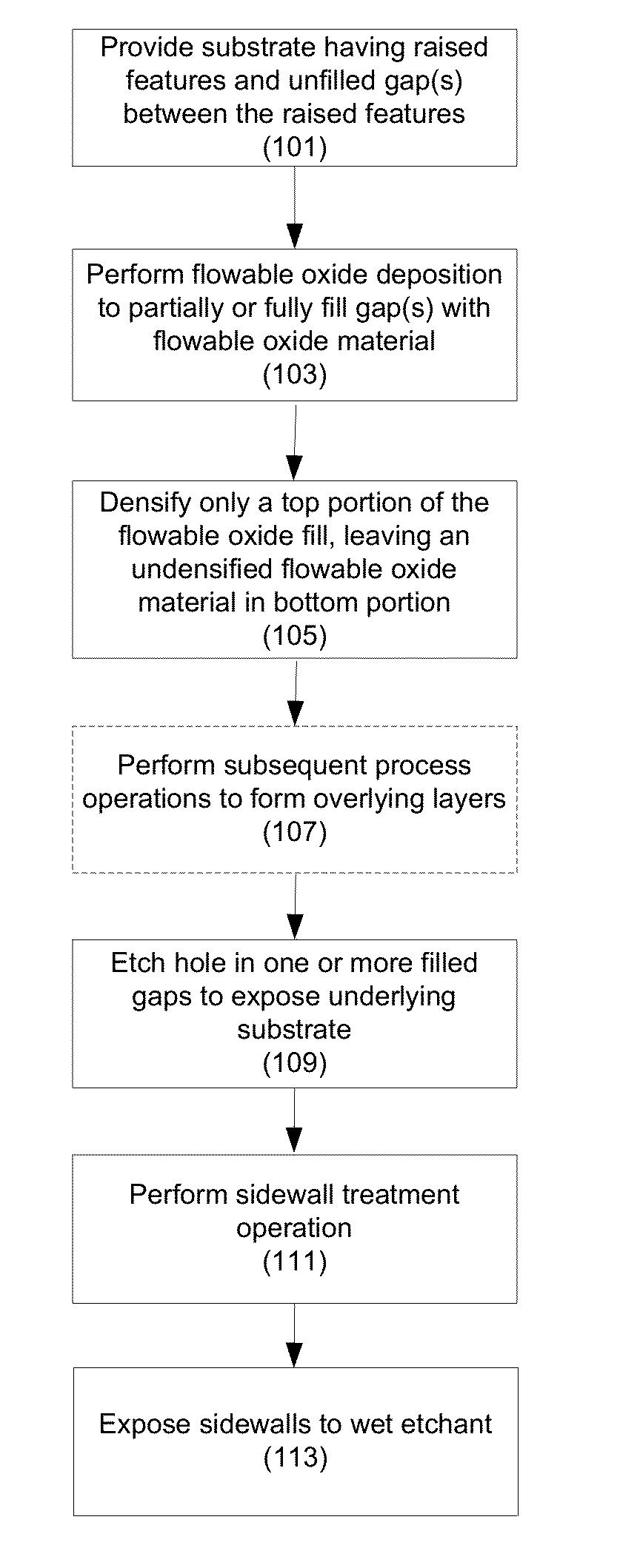
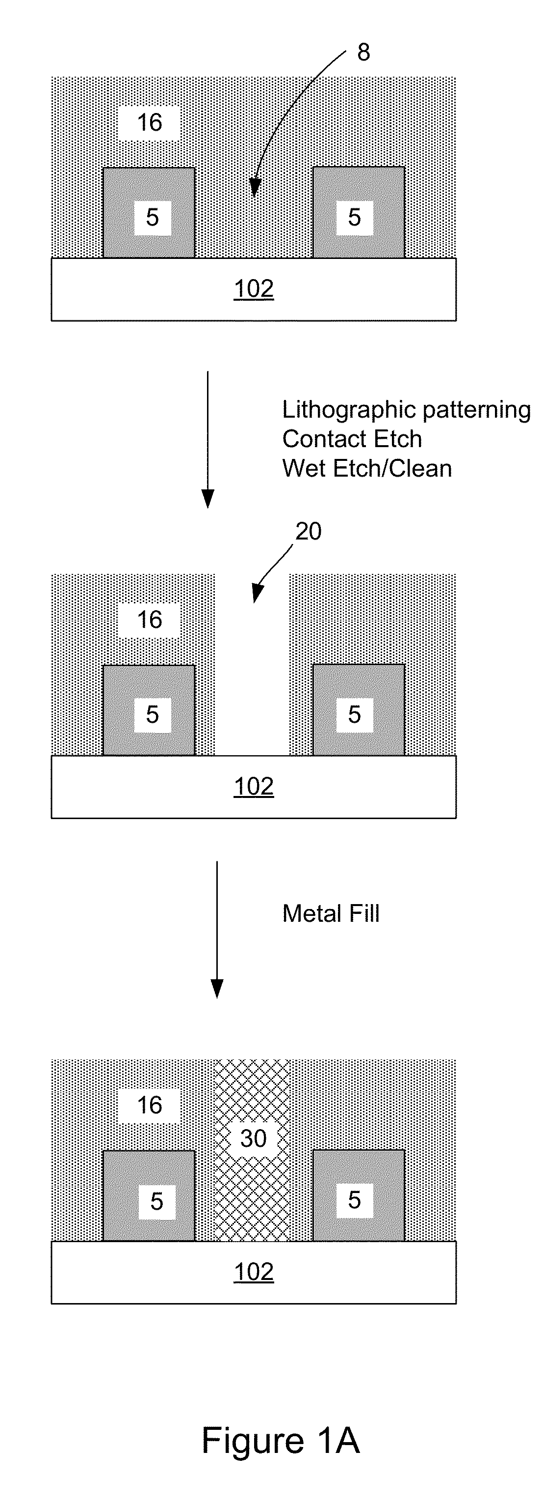
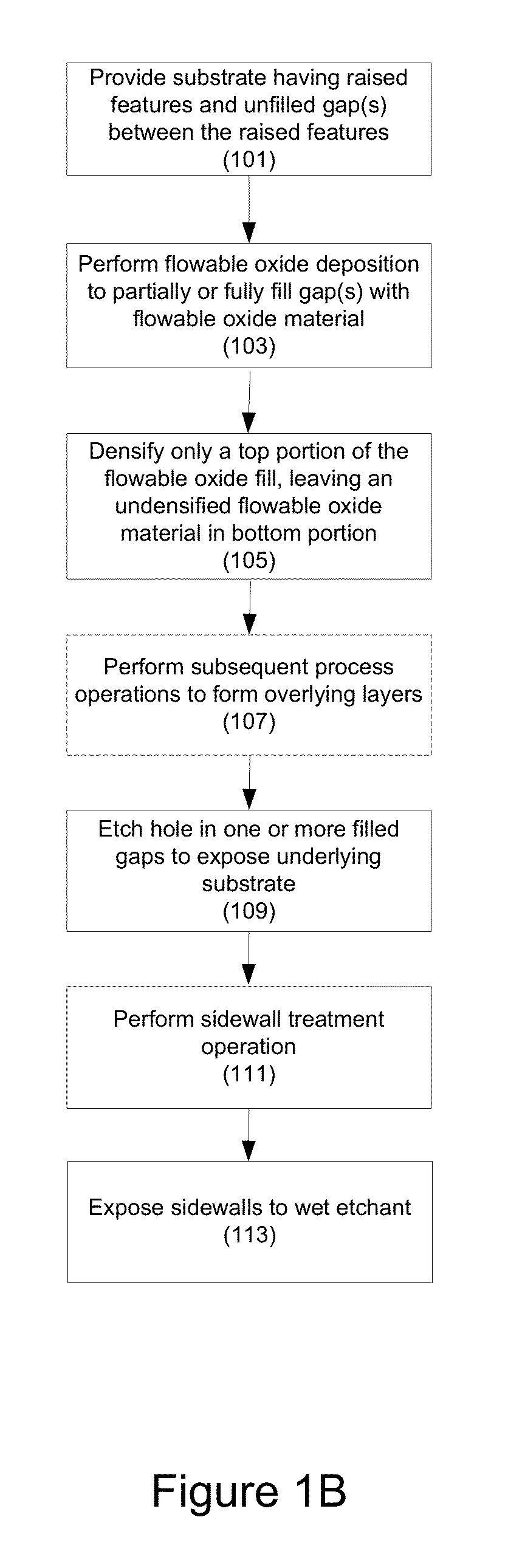
[0028]The present invention pertains to methods of filling gaps on a substrate. In certain embodiments, the methods pertain to filling high aspect (AR) ratio (typically at least 6:1, for example 7:1 or higher), narrow width (e.g., sub-50 nm) gaps. In certain embodiments, the methods pertain filling both low AR gaps (e.g., wide trenches). Also in certain embodiments, gaps of varying AR may be on the substrate, with the embodiments directed at filling low and high AR gaps.

[0029]It is often necessary in semiconductor processing to fill high aspect ratio gaps with insulating material. This is the case for shallow trench isolation (STI), inter-metal dielectric (IMD) layers, inter-layer dielectric (ILD) layers, pre-metal dielectric (PMD) layers, passivation layers, etc. As device geometries shrink and thermal budgets are reduced, void-free filling of narrow width, high aspect ratio (AR) features (e.g., AR>6:1) becomes increasingly difficult due to limitations of existing depos...


PUM


Abstract

Provided herein are novel pre-metal dielectric (PMD) integration schemes. According to various embodiments, the methods involve depositing flowable dielectric material to fill trenches or other gaps between gate structures in a front end of line (FEOL) fabrication process. The flowable dielectric material may be partially densified to form dual density filled gaps having a low density region capped by a high density region. In certain embodiments, the methods include further treating at least a portion of the gap fill material after subsequent process operations such as chemical mechanical planarization (CMP) or contact etching.

Description

CROSS-REFERENCE TO RELATED APPLICATIONS[0001]This application claims benefit under 35 USC 119(e) of the following U.S. Provisional Patent Applications: U.S. Provisional Patent Application No. 61 / 421,548, filed Dec. 9, 2010 and U.S. Provisional Patent Application No. 61 / 492,319, filed Jun. 1, 2011, all of which are incorporated herein by this reference.BACKGROUND OF THE INVENTION[0002]It is often necessary in semiconductor processing to fill high aspect ratio gaps with insulating material. This is the case for shallow trench isolation (STI), inter-metal dielectric (IMD) layers, inter-layer dielectric (ILD) layers, pre-metal dielectric (PMD) layers, passivation layers, etc. As device geometries shrink and thermal budgets are reduced, void-free filling of narrow width, high aspect ratio (AR) features (e.g., AR>6:1) becomes increasingly difficult due to limitations of existing deposition processes.SUMMARY OF THE INVENTION[0003]Provided herein are novel pre-metal dielectric (PMD) inte...

Claims


Application Information

Patent Timeline
IPC IPC(8): H01L21/311H01L21/00
CPCH01L21/311H01L21/00H01L21/0234H01L21/76814H01L21/76801H01L21/02348H01L21/76837H01L21/76825H01L21/76828H01L21/02274H01L21/3105H01L21/76826H01L21/02164H01L21/02126
Inventor DANEK, MICHALVAN SCHRAVENDIJK, BARTDRAEGER, NERISSANITTALA, LAKSHMINARAYANA
Owner NOVELLUS SYSTEMS
Why Eureka
Try Eureka