Diamond sensors, detectors, and quantum devices

a detector and diamond technology, applied in the field of diamond sensors, detectors and quantum devices, can solve the problems of insufficient counting rate, weak single photon emission of quantum spin defects in such materials, and the inability to meet the requirements of expensive and bulky cryogenic cooling apparatus, etc., to improve the coupling between the light source and the point defect, improve the sensitivity and/or directionality of detection, and improve the effect of outcoupling of light from the point d

Active Publication Date: 2014-04-01
ELEMENT SIX LTD
View PDF2 Cites 56 Cited by
  • Summary
  • Abstract
  • Description
  • Claims
  • Application Information

AI Technical Summary

Benefits of technology

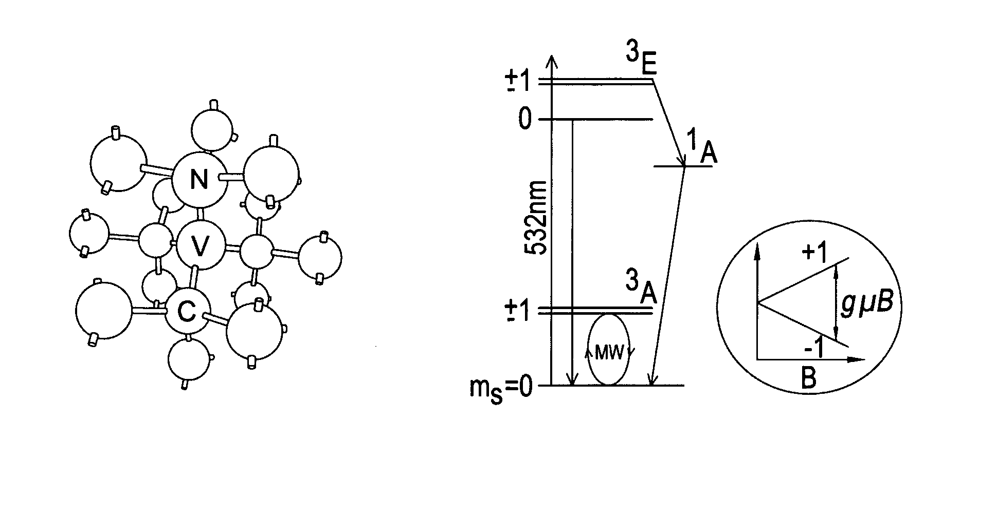
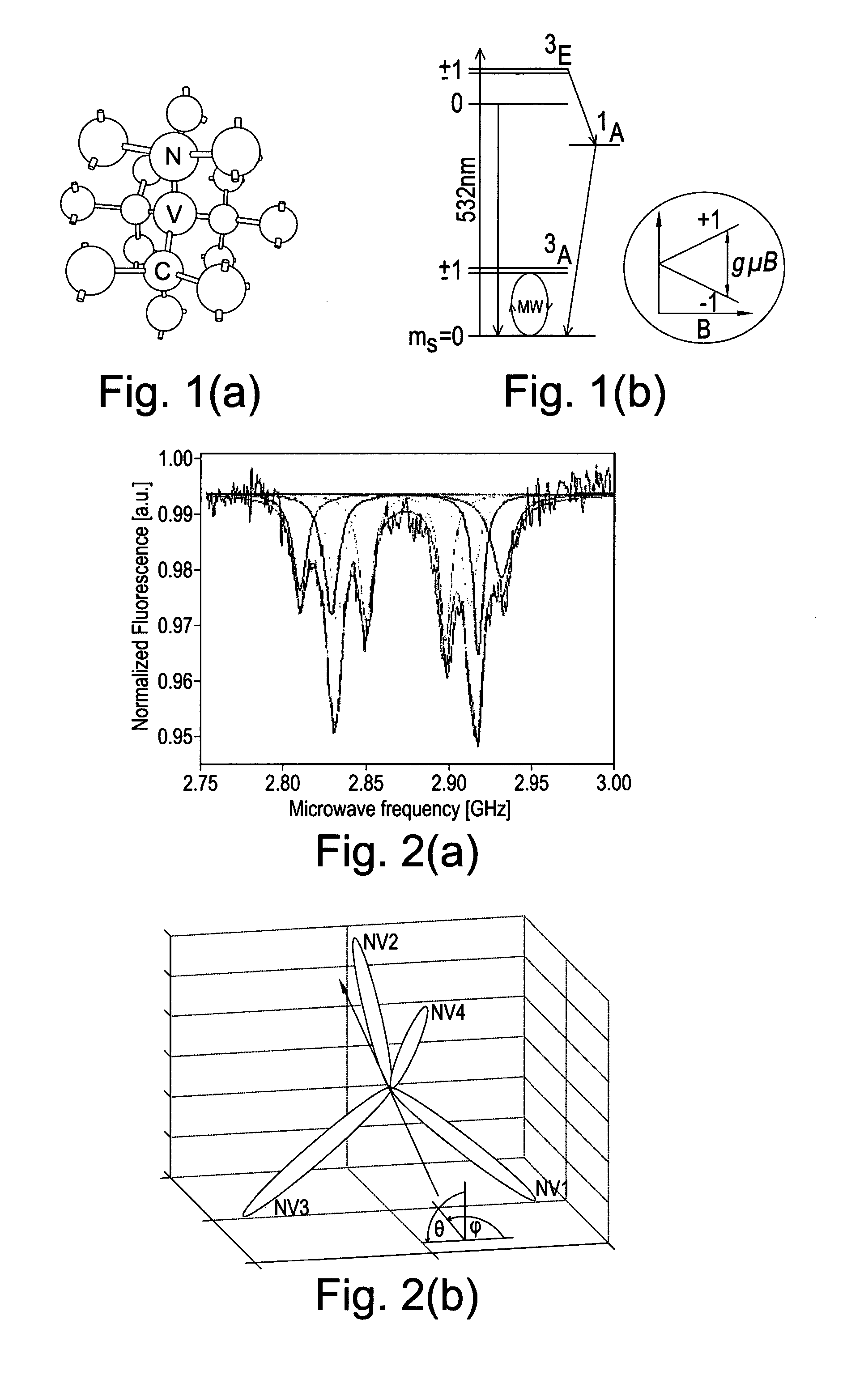
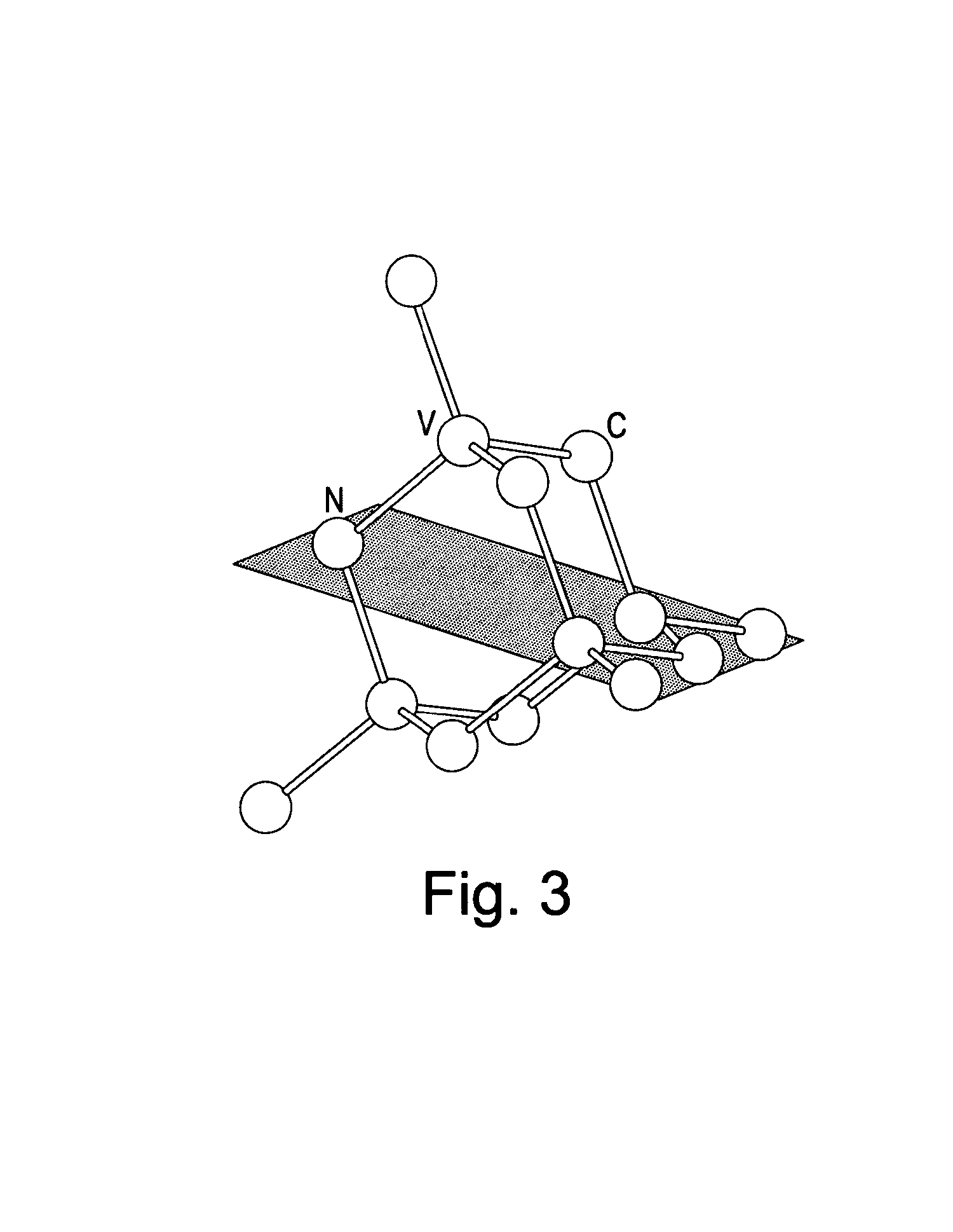
[0018]The present inventors have now found that other point defects in synthetic CVD diamond material can also be preferentially aligned, specifically the NV− defect found to be useful in quantum spin applications as previously described. Furthermore, the present inventors have found that through careful selection of a suitable substrate, careful processing of a growth surface of the substrate, and careful control of the CVD growth conditions a very high degree of point defect alignment can be achieved. Further still, the present inventors have realized that preferential alignment of point defects can be used to increase emission strength and / or light collection from point defects in synthetic CVD diamond material for sensing, detecting, and quantum device applications, increase the sensitivity of point defects in such applications, improve the strength of coupling between point defects, and improve the directionality of the sensing and emissive functionality of the point defects. Such developments can improve the performance of sensing, detecting, and quantum devices and / or aid in simplifying and miniaturizing associated device components required to perform sensing, detecting, and / or processing functionality in conjunction with synthetic CVD diamond material. These realizations allow single crystal synthetic CVD diamond material to be specifically engineered to have highly aligned defects of a desirable type for a particular application. Furthermore, these realizations allow device components to be specifically engineered to optimize the use of preferentially oriented defects. That is, a device configuration can be engineered to make maximum use of the preferential orientation of point defects within the single crystal synthetic CVD diamond material thus improving performance.
[0025]According to a second aspect of the present invention there is provided a synthetic CVD diamond device component for use in a sensing, detecting or quantum spin device, said device component formed of a material as described above. In such a device component, preferably an outcoupling surface or structure is provided having a position and orientation which is formed relative to the preferentially aligned point defects to improve outcoupling of light from the point defects.
[0026]According to a third aspect of the present invention there is provided a device comprising a device component as described above. The device may comprise a light source for optically pumping one or more of the plurality of preferentially aligned point defects in the single crystal synthetic CVD diamond material. The light source may be oriented relative to the preferentially aligned point defects so as to improve coupling between the light source and the point defects.
[0027]The device may optionally comprise further components configured to interact with the preferentially aligned point defects. For example, the device may comprise a detector for detecting emission from one or more preferentially aligned point defects in the single crystal synthetic CVD diamond material. The detector may be positioned and oriented relative to the one or more preferentially oriented point defects to improve sensitivity and / or directionality of detection.
[0029]The device may optionally form a micro fluidic device comprising a micro fluidic channel for receiving a fluid sample, the single crystal synthetic CVD diamond material being located adjacent the microfluidic channel. The microfluidic channel and the point defects may be oriented relative to each other to improve coupling between the fluid sample and the point defects in the single crystal synthetic CVD diamond material.

Problems solved by technology

This can negate the requirement for expensive and bulky cryogenic cooling apparatus for certain applications where miniaturization is desired.
One major problem in producing materials suitable for quantum applications is preventing quantum spin defects from decohering, or at least lengthening the time a system takes to decohere (i.e. lengthening the “decoherence time”).
One problem with quantum materials is that single photon emission from quantum spin defects in such materials can be very weak.
Such counting rates might be insufficient for the realization of advanced QIP protocols based on coupling between spin states and optical transitions within reasonable data acquisition times.
In addition to the problem of weak emission, it is evident that the high refractive index of diamond material means that due to total internal reflection very few photons can be collected within a small solid angle.
While such problems have been discussed above in relation to the NV− defect it will be appreciated that similar problems are also evident for other point defects within synthetic diamond material.

Method used


Image

  • Diamond sensors, detectors, and quantum devices
  • Diamond sensors, detectors, and quantum devices
  • Diamond sensors, detectors, and quantum devices

Examples


example 1

D2d

[0068]In a crystal with Td symmetry there are three possible symmetry related sites (orientations) of a defect with D2d symmetry. If all symmetry related sites are equally probably then the defect is randomly oriented.

[0069]If the probability of finding one particular site is n (where 0≦n≦1) and that for each of the other two (1−n) / 2 then the degree of preferential orientation can vary between completely preferentially oriented (n=1; 100% preferentially aligned), randomly oriented (n=⅓; 0% preferentially aligned) to oriented with equal probability in only two of the three possible symmetry related sites (n=0).

[0070]If the probabilities of occupancy of the three possible symmetry related sites are all different, say n, (1−n−p) / 2 and (1−n+p) / 2 then all possibilities for different distributions amongst the three symmetry related sites are bounded by the lines 0≦n≦1, p≧0 and n+p≦1.

example 2

C3v

[0071]Four directions along which the trigonal axis of a symmetry related site can be oriented: [111], [ 111], [1 11] and [ 11 1] (and their inverses if the defect does not posses inversion symmetry) and labelled a, b, c, d

[0072]Consider growth direction along [001]:

[0073]The symmetry axes of the sites (a), (b), (c) and (d) make equal angles with respect to the growth direction (arccos(√{square root over (⅓)})). No preferential orientation (0% preferential alignment) of trigonal defects is expected for growth along the [001]. The same argument applies for growth along all 100 directions.

[0074]Consider growth direction along [110]:

[0075]The symmetry axes of the sites (a) and (b) make equal angles with respect to the growth direction (arccos(√{square root over (⅔)})). The symmetry axes of the sites (c) and (d) make equal angles with respect to the growth direction (90°).

[0076]Thus sites (a) and (b) can be treated as equivalent and sites (c) and (d) treated as equivalent.

[0077]If t...

synthesis example

[0143]A synthetic type Ib HPHT diamond plate with a pair of approximately parallel major faces within approximately 5° of (001) was selected. The plate was fabricated into a square substrate suitable for homoepitaxial synthesis of single crystal CVD diamond material by a process including the following steps:

i) laser cutting of the substrate to produce a plate with all edges;

[0144]ii) lapping and polishing the major surface upon which growth is to occur, the lapped and polished part having dimensions about 4.0 mm×4.0 mm by 300 μm thick, with all faces {100}. The defect level at or below the substrate surface is minimised by careful preparation of the substrate as disclosed in EP 1 292 726 and EP 1 290 251. It is possible to reveal the defect levels being introduced by this processing by using a revealing plasma etch. It is possible routinely to produce substrates in which the density of defects measurable after a revealing etch is dependent primarily on the material quality and is ...


PUM

PropertyMeasurementUnit
decoherence time T2aaaaaaaaaa

Abstract

A single crystal synthetic CVD diamond material comprising: a growth sector; and a plurality of point defects of one or more type within the growth sector, wherein at least one type of point defect is preferentially aligned within the growth sector, wherein at least 60% of said at least one type of point defect shows said preferential alignment, and wherein the at least one type of point defect is a negatively charged nitrogen-vacancy defect (NV−).

Description

FIELD OF INVENTION[0001]The present invention relates to synthetic chemical vapour deposited (CVD) diamond material for use in sensing, detecting and quantum processing applications.BACKGROUND OF INVENTION[0002]Point defects in synthetic diamond material, particularly quantum spin defects and / or optically active defects, have been proposed for use in various sensing, detecting, and quantum processing applications including: magnetometers; spin resonance devices such as nuclear magnetic resonance (NMR) and electron spin resonance (ESR) devices; spin resonance imaging devices for magnetic resonance imaging (MRI); and quantum information processing devices such as for quantum computing.[0003]Many point defects have been studied in synthetic diamond material including: silicon containing defects such as silicon-vacancy defects (Si-V), silicon di-vacancy defects (S1-V2), silicon-vacancy-hydrogen defects (Si-V:H), silicon di-vacancy hydrogen defects (S-V2:H); nickel containing defect; chr...

Claims


Application Information

Patent Timeline
Patent Type & Authority Patents(United States)
IPC IPC(8): B82Y20/00
CPCC30B29/04C30B25/105C01B32/25C23C16/27
Inventor TWITCHEN, DANIEL JAMESMARKHAM, MATTHEW LEE
Owner ELEMENT SIX LTD
Why Eureka
Try Eureka