Bonding surfaces for direct bonding of semiconductor structures

a technology of direct bonding and semiconductor structure, which is applied in the direction of semiconductor/solid-state device details, semiconductor devices, electrical apparatus, etc., can solve the problems of inability to meet the requirements of the application, the direct bonding process may be undesirable, and the direct metal-to-metal bonding between active conductive features of the semiconductor structure may be prone to mechanical failure or electrical failure in some instances

Inactive Publication Date: 2014-04-15
SONY SEMICON SOLUTIONS CORP
View PDF9 Cites 99 Cited by
  • Summary
  • Abstract
  • Description
  • Claims
  • Application Information

AI Technical Summary

Problems solved by technology

For example, some direct metal-to-metal bonding methods are carried out at relatively high temperatures resulting in at least partial melting of the metal material at the bonding interface.
Such direct bonding processes may be undesirable for use in bonding processed semiconductor structures that include one or more device structures, as the relatively high temperatures may adversely affect the earlier formed device structures.
Direct metal-to-metal bonds between active conductive features in semiconductor structures may, in some instances, be prone to mechanical failure or electrical failure after a period of time even though an acceptable direct metal-to-metal bond may be initially established between the conductive features of the semiconductor structures.

Method used


Image

  • Bonding surfaces for direct bonding of semiconductor structures
  • Bonding surfaces for direct bonding of semiconductor structures
  • Bonding surfaces for direct bonding of semiconductor structures

Examples


embodiment 1

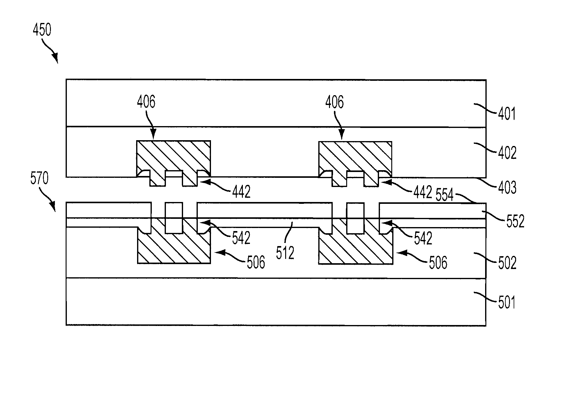
[0115] A method of directly bonding a first semiconductor structure to a second semiconductor structure, comprising: providing a first semiconductor structure comprising: at least one device structure comprising a conductive material, the at least one device structure exposed at a bonding surface of the first semiconductor structure; and a dielectric material exposed at the bonding surface of the first semiconductor structure, the dielectric material disposed adjacent the at least one device structure of the first semiconductor structure, an exposed surface of the dielectric material at the bonding surface of the first semiconductor structure defining a bond plane of the first semiconductor structure; causing the at least one device structure of the first semiconductor structure to project a distance from the bond plane of the first semiconductor structure beyond the adjacent dielectric material; providing a second semiconductor structure comprising: at least one device structure co...

embodiment 2

[0116] The method of Embodiment 1, wherein causing the at least one device structure of the first semiconductor structure to project the distance from the bond plane of the first semiconductor structure beyond the adjacent dielectric material comprises removing a portion of the dielectric material from the first semiconductor structure.

embodiment 3

[0117] The method of Embodiment 2, wherein removing the portion of the dielectric material from the first semiconductor structure comprises etching the dielectric material.


PUM


Abstract

Methods of directly bonding a first semiconductor structure to a second semiconductor structure include directly bonding at least one device structure of a first semiconductor structure to at least one device structure of a second semiconductor structure in a conductive material-to-conductive material direct bonding process. In some embodiments, at least one device structure of the first semiconductor structure may be caused to project a distance beyond an adjacent dielectric material on the first semiconductor structure prior to the bonding process. In some embodiments, one or more of the device structures may include a plurality of integral protrusions that extend from a base structure. Bonded semiconductor structures are fabricated using such methods.

Description

TECHNICAL FIELD[0001]The present invention relates to methods of directly bonding together semiconductor structures, and to bonded semiconductor structures formed using such methods.BACKGROUND[0002]The three-dimensional (3D) integration of two or more semiconductor structures can produce a number of benefits to microelectronic applications. For example, 3D integration of microelectronic components can result in improved electrical performance and power consumption while reducing the area of the device foot print. See, for example, P. Garrou, et al., “The Handbook of 3D Integration,” Wiley-VCH (2008).[0003]The 3D integration of semiconductor structures may take place by the attachment of a semiconductor die to one or more additional semiconductor dies (i.e., die-to-die (D2D)), a semiconductor die to one or more semiconductor wafers (i.e., die-to-wafer (D2W)), as well as a semiconductor wafer to one or more additional semiconductor wafers (i.e., wafer-to-wafer (W2W)), or a combination...

Claims


Application Information

Patent Timeline
Patent Type & Authority Patents(United States)
IPC IPC(8): H01L21/00
CPCH01L2224/0391H01L2224/05571H01L2224/05666H01L2224/05624H01L2224/03616H01L2224/05684H01L23/48H01L2224/03452H01L24/05H01L24/80H01L2224/80097H01L2224/08147H01L23/3178H01L2224/05681H01L2224/80895H01L2224/80986H01L2224/05647H01L2224/05572H01L2224/05557H01L2224/03845H01L2224/05671H01L2224/0345H01L2224/80365H01L2224/80357H01L2224/80896H01L24/03H01L2224/03831H01L2224/05573H01L2924/00014H01L2224/08148H01L2224/0807H01L2224/8034H01L2224/80141H01L2224/08145H01L2924/00012H01L2924/20105H01L2224/05552
Inventor SADAKA, MARIAM
Owner SONY SEMICON SOLUTIONS CORP
Why Eureka
Try Eureka