Method of producing circuit board, and circuit board obtained using the manufacturing method

a manufacturing method and circuit board technology, applied in the direction of printed circuit assembling, metallic pattern materials, chemical vapor deposition coating, etc., can solve the problems of short circuiting or migration between the wirings that can easily occur, the production cost is disadvantageously high, and the metal from the removed portions is wasted

Inactive Publication Date: 2014-04-15
PANASONIC CORP
View PDF56 Cites 3 Cited by
  • Summary
  • Abstract
  • Description
  • Claims
  • Application Information

AI Technical Summary

Benefits of technology

[0017]It is an object of the present invention to provide a method of producing a circuit substrate that makes it possible to form a high-precision electric circuit on an insulative substrate in an easy manner.

Problems solved by technology

In circuit wirings of increased density, short circuiting or migration between the wirings can easily occur.
With such a method, the metal from the removed portions is wasted and therefore the production cost is disadvantageously high.
As a result, the following problem is encountered.

Method used


Image

  • Method of producing circuit board, and circuit board obtained using the manufacturing method
  • Method of producing circuit board, and circuit board obtained using the manufacturing method
  • Method of producing circuit board, and circuit board obtained using the manufacturing method

Examples


first embodiment

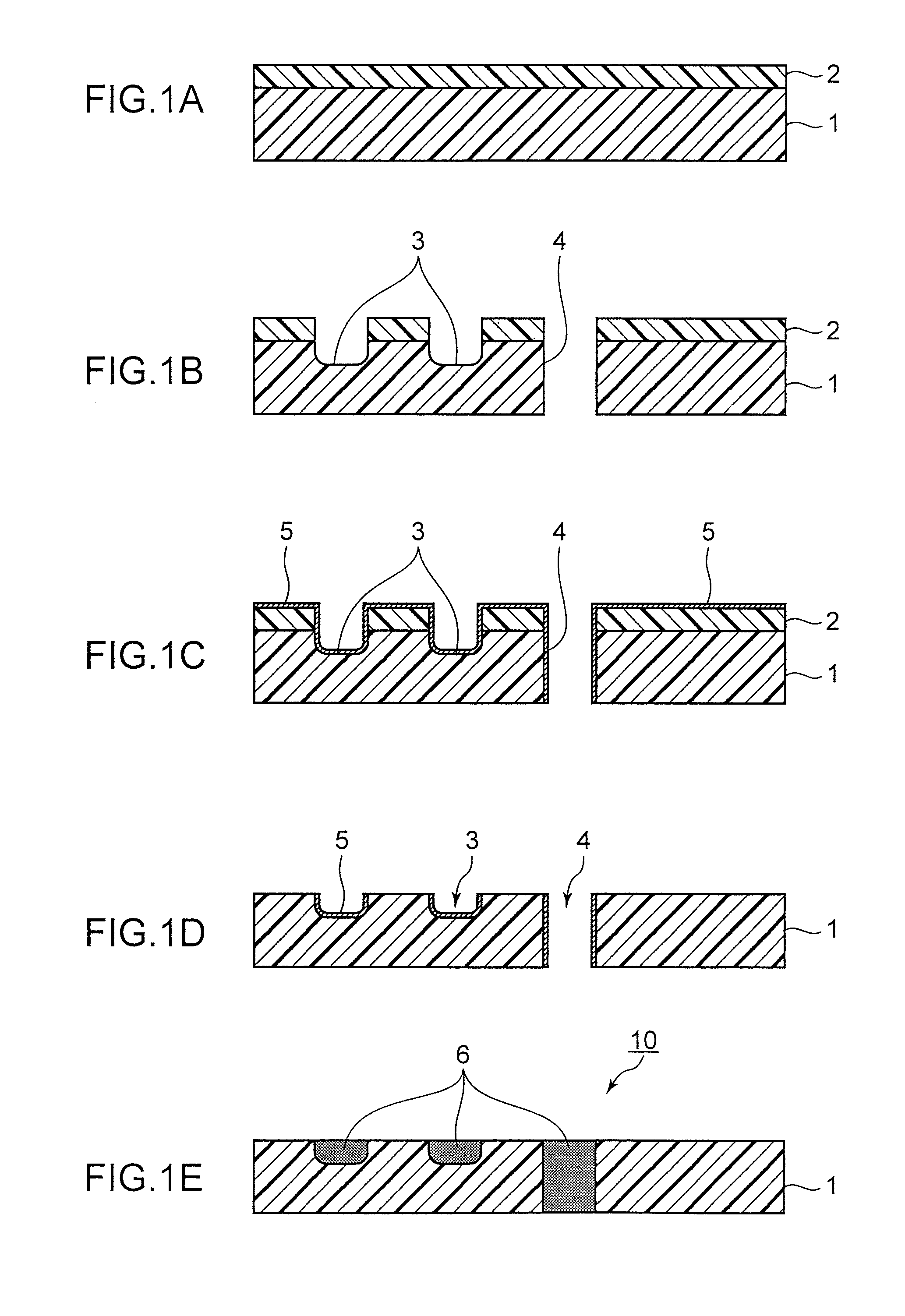
[0029]The method of producing a circuit board according to the present embodiment includes a film-forming step of forming a resin film on a surface of an insulative substrate; a circuit pattern-forming step of forming a circuit pattern portion by forming a recessed portion having a depth equal to or greater than a thickness of the resin film, with an outer surface of the resin film serving as a reference; a catalyst-depositing step of depositing a plating catalyst or a precursor thereof on a surface of the circuit pattern portion and a surface of the resin film; a film-separating step of removing the resin film from the insulative substrate; and a plating step of forming an electroless plating film only in a region where the plating catalyst or the precursor thereof remains after the resin film is separated.

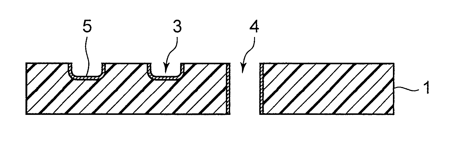
[0030]First, the method of producing a circuit board according to the first embodiment of the present invention will be described. FIGS. 1A to 1E are schematic cross-sectional vi...

second embodiment

[0125]In the first embodiment, a circuit board is explained that is obtained by forming an electric circuit on a flat insulative substrate, but the present invention is not limited to such a configuration. More specifically, a circuit board (steric circuit board) provided with an electric circuit with accurate wiring can be also obtained by using an insulative substrate of a three-dimensional shape such that has a stepwise steric surface as the aforementioned insulative substrate.

[0126]A method of producing a steric circuit board according to the second embodiment will be explained below.

[0127]FIGS. 4A to 4E are schematic cross-sectional views illustrating each step of the process of producing a steric circuit board according to the second embodiment.

[0128]First, a resin film 2 is formed on the surface of a steric insulative substrate 51 having a stepwise portion as shown in FIG. 4A. This step corresponds to a film-forming step.

[0129]Various resin molded bodies such that can be used...

example 1

[0138]A film of a styrene-butadiene copolymer (SBR) with a thickness of 2 μm was formed on the surface of an epoxy resin base material R1766 manufactured by Panasonic Electric Works Co., Ltd. with a thickness of 100 μm. The film was formed by coating a methyl ethyl ketone (MEK) suspension (manufactured by Japan Zeon Co., Ltd., acid equivalent 600, particle diameter 200 nm, content ratio of solids 15%) of the styrene-butadiene copolymer (SBR) on the surface of the epoxy resin base material and drying for 30 min at a temperature of 80° C.

[0139]The epoxy resin base material having the film formed thereon was then subjected to groove formation processing of forming grooves of substantially rectangular cross section with a thickness of 20 μm and a depth of 30 μm by laser processing. A MODEL 5330 equipped with a UV-YAG laser and manufactured by ESI was used for the laser processing.

[0140]The epoxy resin base material having the groove formed therein was dipped into a cleaner conditioner (...


PUM


Abstract

One aspect of the present invention resides in a method of producing a circuit board, including a film-forming step of forming a resin film on a surface of an insulative substrate; a circuit pattern-forming step of forming a circuit pattern portion by forming a recessed portion having a depth equal to or greater than a thickness of the resin film, with an outer surface of the resin film serving as a reference; a catalyst-depositing step of depositing a plating catalyst or a precursor thereof on a surface of the circuit pattern portion and a surface of the resin film; a film-separating step of removing the resin film from the insulative substrate; and a plating step of forming an electroless plating film only in a region where the plating catalyst or the precursor thereof remains after the resin film is separated.

Description

[0001]This application is a National Stage Application of International Application No. PCT / JP2009 / 070106, filed Nov. 30, 2009, which is a continuation-in-part of U.S. application Ser. No. 12 / 326,169, filed on Dec. 2, 2008, and claims priority to Japanese Application No. 2009-251269, filed Oct. 30, 2009, the disclosures of which are expressly incorporated herein by reference in their entireties.TECHNICAL FIELD[0002]The present invention relates to a method of producing a circuit board and to a circuit board obtained using the manufacturing method.BACKGROUND ART[0003]The level of functionality of electric devices such as portable information terminal devices such as cellular phones, computers and peripheral equipment thereof, and various home information products has been rapidly increasing. Accordingly, circuit boards that are carried in such electric devices are required to have an even higher density of electric circuits. Methods that can form accurately the wiring of electric cir...

Claims


Application Information

Patent Timeline
Patent Type & Authority Patents(United States)
IPC IPC(8): H05K1/03
CPCH05K3/184H05K2201/09736H05K2203/0769H05K2203/0264H05K2203/0565H05K3/0014H05K2203/0108H05K2201/0133H05K3/107H05K1/0284H05K3/0032Y10T29/49124Y10T29/49126Y10T29/49128Y10T29/4913Y10T29/49155
Inventor YOSHIOKA, SHINGOFUJIWARA, HIROAKI
Owner PANASONIC CORP
Why Eureka
Try Eureka