Semiconductor light emitting device

a technology of light-emitting devices and semiconductors, which is applied in the direction of semiconductor devices, basic electric elements, electrical equipment, etc., can solve the problem of fast deterioration at a pla

Active Publication Date: 2014-04-22
TOYODA GOSEI CO LTD
View PDF4 Cites 19 Cited by
  • Summary
  • Abstract
  • Description
  • Claims
  • Application Information

AI Technical Summary

Benefits of technology

[0014]In the semiconductor light emitting device according to a third aspect, the closest inter-electrode distance is a distance between a separated electrode portion of the first polarity and the conductive portion of the second polarity. Since the distance between the separated electrode portion of the first polarity and the conductive portion (which includes the separated electrode portion, the wiring, the pad electrode and the like) of the second polarity is narrower at the peripheral portion, the light emission intensity distribution in the light emission surface of the semiconductor light emitting device is more uniform, compared to the light emission intensity distribution of the conventional semiconductor light emitting device.
[0015]In the semiconductor light emitting device according to a fourth aspect, each of the conductive portion of the first polarity and the conductive portion of the second polarity includes a plurality of the separated electrode portions. The closest inter-electrode distance is a distance between the separated electrode portion of the conductive portion of the first polarity and the separated electrode portion of the conductive portion of the second polarity. Since the distance between the separated electrode portion of the first polarity and the separated electrode portion of the second polarity is narrower at the peripheral portion, the light emission intensity distribution in the light emission surface of the semiconductor light emitting device is more uniform, compared to the light emission intensity distribution of the conventional semiconductor light emitting device.
[0021]The semiconductor light emitting device according to a tenth aspect, the conductive portion of the first polarity includes the separated electrode portions of the first polarity. The closest inter-electrode distance is a distance between the separated electrode portions of the first polarity. The reason is as follows: also in a flip chip having a planar electrode portion of a plane shape, the distance between the separated electrode portions of the same polarity is made to be narrower at the peripheral portion, so that the light emission intensity distribution in the light emission surface becomes more uniform.

Problems solved by technology

When a current density on the light emission surface of a semiconductor layer is non-uniform, the deterioration progresses fast at a place at which large current flows.

Method used


Image

  • Semiconductor light emitting device
  • Semiconductor light emitting device
  • Semiconductor light emitting device

Examples


Embodiment Construction

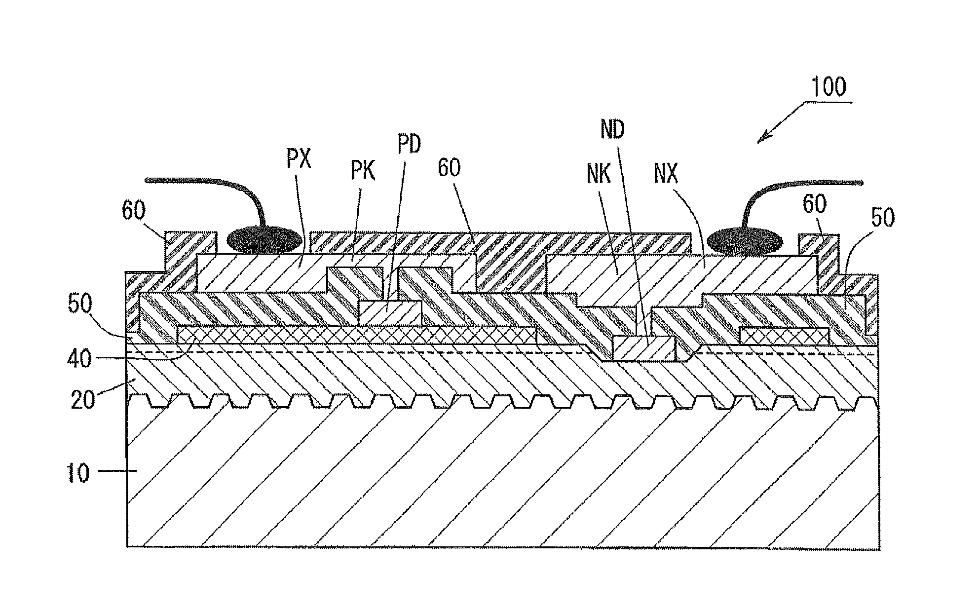
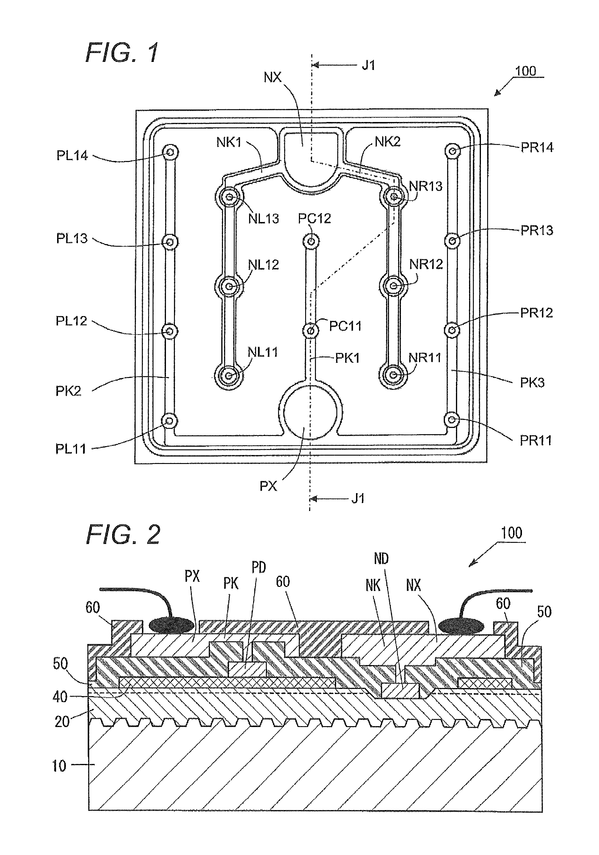
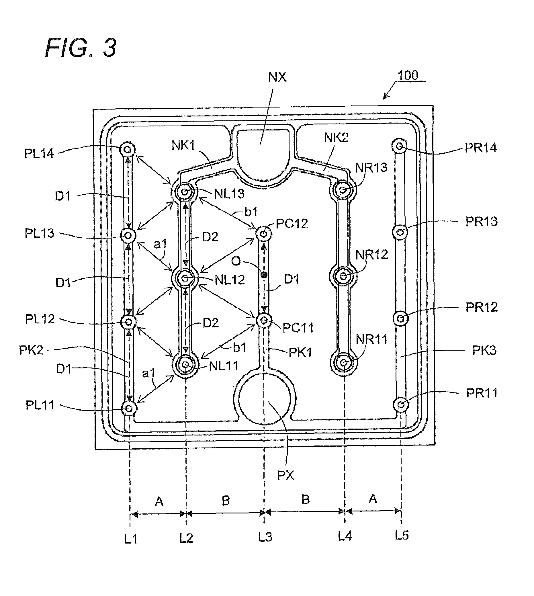
[0036]Hereinafter, specific illustrative embodiments of the invention will be described with reference to the drawings while exemplifying a semiconductor light emitting device. However, the invention is not limited to the illustrative embodiments. That is, the invention can be applied to a light emitting device in which at least a part of p auxiliary electrodes and n auxiliary electrodes are separately (discretely) arranged. Also, a stacked structure of respective layers and an electrode structure in the light emitting device that will be described later are just exemplary. It doesn't matter whether a stacked structure is different from those of the illustrative embodiments. In the respective drawings, a thickness of each layer is conceptually shown and does not indicate an actual thickness.

First Illustrative Embodiment

[0037]1. Semiconductor Light Emitting Device

[0038]A semiconductor light emitting device of this illustrative embodiment is described. FIG. 1 is a plan view of a light...


PUM


Abstract

A semiconductor light emitting device includes: a first conductivity type semiconductor layer; a light emission layer; a second conductivity type semiconductor layer; a conductive portion of a first polarity electrically connected to the first conductivity type semiconductor layer; and a conductive portion of a second polarity electrically connected to the second conductivity type semiconductor layer. At least one of the conductive portion of the first polarity and the conductive portion of the second polarity includes a plurality of separated electrode portions arranged on a light emission surface. The closer the positions of the separated electrode portions are to a center point of the light emission surface, the separated electrode portions are provided sparsely, and the farther the positions of the separated electrode portions are from a center point of the light emission surface, the separated electrode portions are provided densely.

Description

BACKGROUND[0001]1. Technical Field[0002]The invention relates to a semiconductor light emitting device. More specifically, the invention relates to a semiconductor light emitting device having improved amount of emitted light.[0003]2. Background Art[0004]In a semiconductor light emitting device, it is preferable that a luminance distribution on a light emission surface of a light emission layer is uniform. When a current density on the light emission surface of a semiconductor layer is non-uniform, the deterioration progresses fast at a place at which large current flows. Also, the more uniform the current density on the light emission surface, the light emitted from the semiconductor light emitting device becomes brighter.[0005]Therefore, a technology for making the luminance on the light emission surface uniform has been developed. For example, Patent Document 1 discloses a semiconductor light emitting device including electrodes having linear portions arranged at an equal interva...

Claims


Application Information

Patent Timeline
Patent Type & Authority Patents(United States)
IPC IPC(8): H01L33/00H01L33/36
CPCH01L2224/48463H01L33/36H01L33/38H01L2224/49107H01L24/06H01L2224/02166H01L2224/04042
Inventor KAMIYA, MASAOKAYAMOTO, KEISUKESAITO, HITOMINODA, HISANOBU
Owner TOYODA GOSEI CO LTD
Why Eureka
Try Eureka