Semiconductor device and method of manufacturing the same

a semiconductor and device technology, applied in semiconductor devices, semiconductor/solid-state device details, electrical apparatus, etc., can solve the problems of defective soldering, heat is not sufficiently transferred to the solder bumps separated from the soldering is difficult to print on the receiving land of the mounting board, so as to suppress defective soldering during reflowing and improve the cleaning characteristics of flux cleaning. , the effect of defective soldering in a narrow array pitch during

Active Publication Date: 2009-03-12
GK BRIDGE 1
View PDF2 Cites 15 Cited by
  • Summary
  • Abstract
  • Description
  • Claims
  • Application Information

AI Technical Summary

Benefits of technology

[0024]According to the present invention, since the height of the solder protruded electrode after reflow heating increases to more than the tolerance for the height of the solder protruded electrode before reflowing so that the solder protruded electrode contacts the receiving land of the mounting board, defective soldering during reflowing can be suppressed.
[0025]As a secondary effect, since the distance between the semiconductor device and the mounting board after reflow heating is widened, cleaning characteristics in flux cleaning are improved, and a gap can be easily sealed by an under-fill resin.
[0026]According to the present invention, since the solder protruded electrode has a shape not extended in the direction facing the adjoining solder protruded electrodes, having the same width as the underlying electrode, but extended in the direction perpendicular to the array direction of the solder protruded electrodes along the insulating protective film, and the quantity of solder can be freely adjusted without widening the pitch distance to the adjoining solder protruded electrodes, defective soldering in a narrow array pitch during reflowing can be suppressed.
[0027]According to the present invention, since the height of the solder protruded electrode after reflow heating can be freely adjusted by adjusting the size of the region extended along the insulating protective film of the solder protruded electrode, defective soldering can be more reliably suppressed by the height-elevating effect of the solder protruded electrode when solder is melted.
[0028]According to the present invention, since the plurality of solder protruded electrodes are provided with the array pitch narrowed as a whole, by disposing the solder protruded electrodes having a triangular plate-like shape in two rows, and by positioning one of the apexes of the solder protruded electrodes in one of the rows between the apexes of two adjacent solder protruded electrodes in the other row, the array distance of the solder protruded electrodes can be narrowed compared with the case where the solder protruded electrodes are linearly disposed in one row.
[0029]Also according to the present invention, the quantity of solder in the solder protruded electrodes can be delicately adjusted by forming dents on surfaces of the solder protruded electrodes. Furthermore, when the semiconductor device is electrically tested, the stable tests of the solder protruded electrodes can be conducted by inserting a probe having a spherical tip into the dents.

Problems solved by technology

Furthermore, since a receiving land provided on a mounting board is 100 μm or less square, solder printing on the receiving land of the mounting board is difficult.
At the same time, if the heights of solder bumps vary, disadvantageously, defective soldering is likely to occur.
Specifically, if there is a portion where the solder bumps do not contact the receiving land of the mounting board due to the variation of the heights of the solder bumps, even if reflow heating is performed, heat is not sufficiently transferred to the solder bumps separated from the receiving land of the mounting board.
Therefore, solder may not be melted to cause poor characteristics, and the shape of the solder may be deformed to cause poor appearance.
However, since solder bumps are formed by a plating process, the above-described semiconductor device has a problem of the variation in the height of bumps, and the variation in the height of the completed bumps tends to be large as the plating resist film is thicker.
With solder bumps having a height of not more than 100 μm, the receiving land of the mounting board is too small to perform solder printing.
Therefore, since heat is not transferred if reflow heating is performed in the state where the solder bumps are isolated from the receiving land, disadvantageously, solder is not melted to cause defective connection, and only a part of solder bumps are melted to make the bump shape abnormal.

Method used


Image

  • Semiconductor device and method of manufacturing the same
  • Semiconductor device and method of manufacturing the same
  • Semiconductor device and method of manufacturing the same

Examples


first embodiment

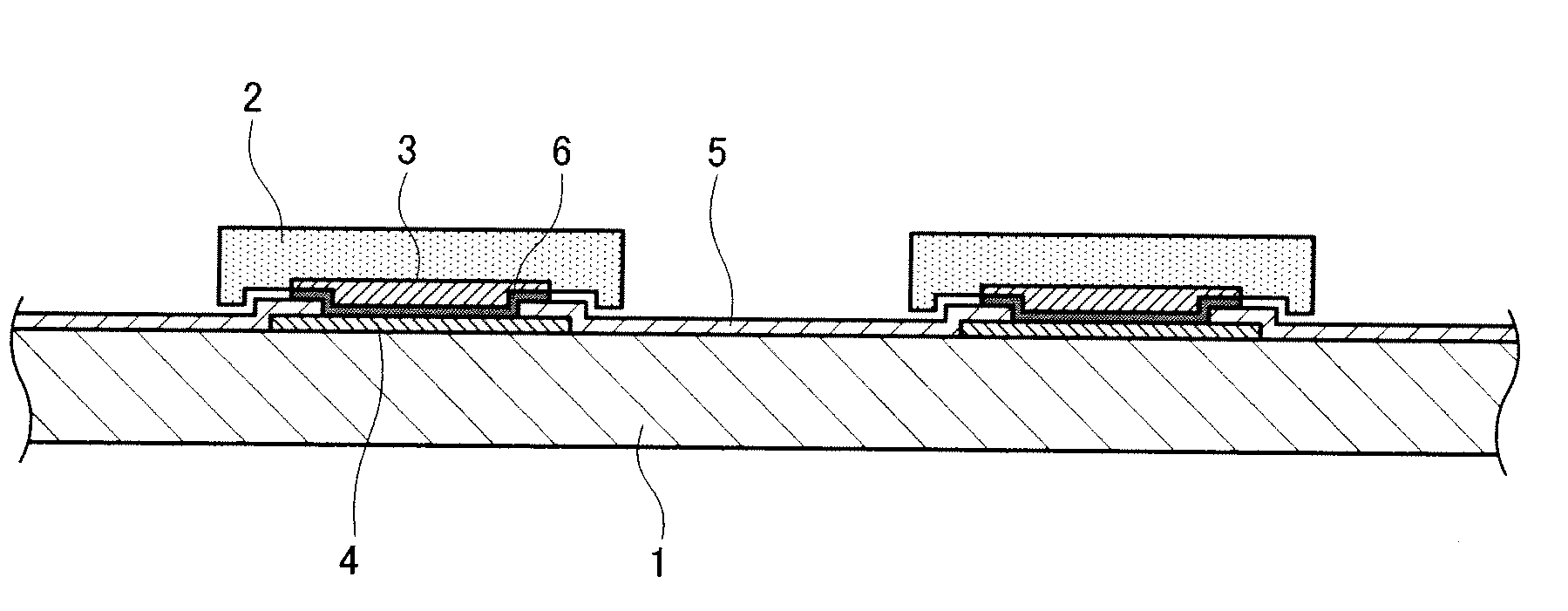
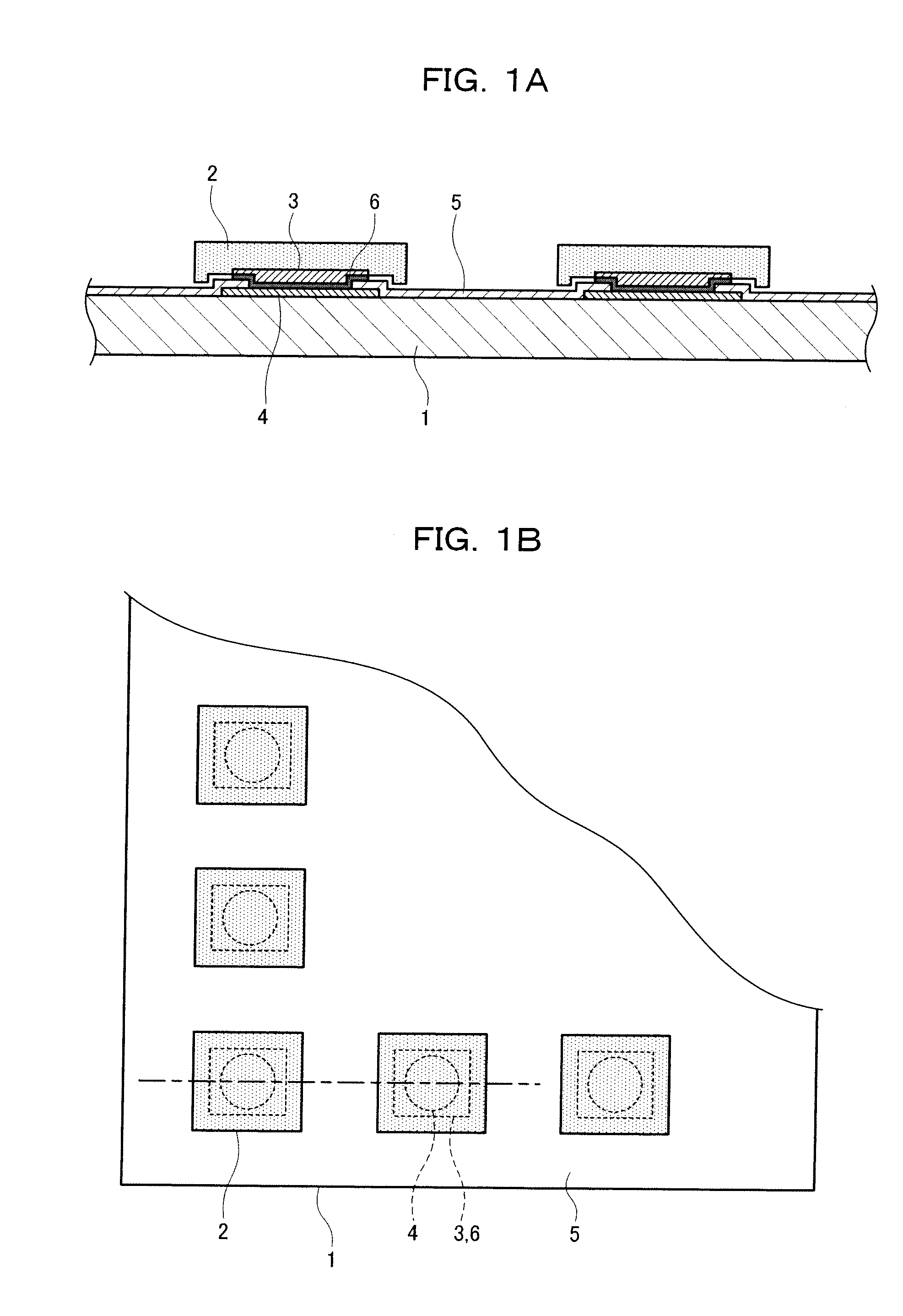
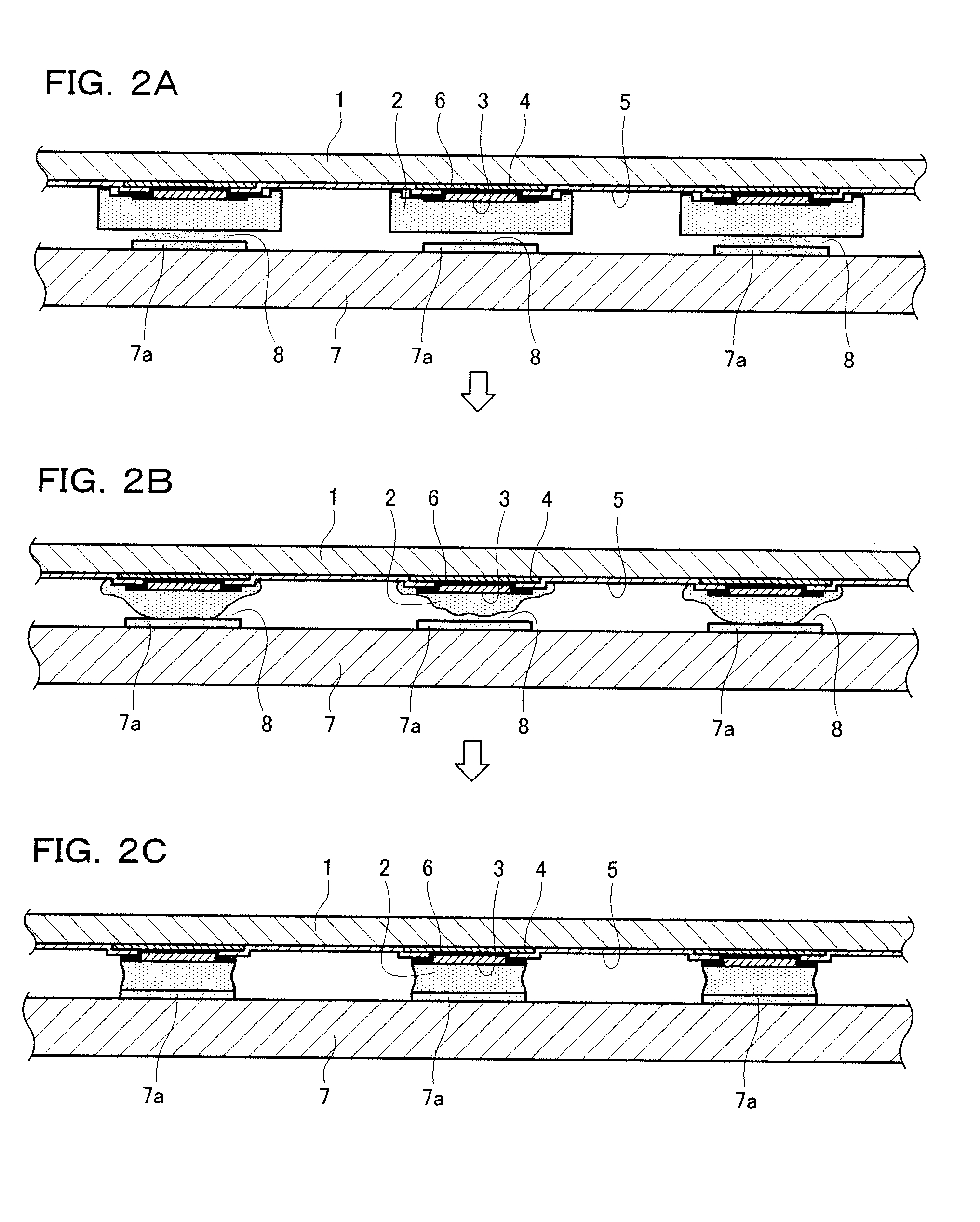
[0047]FIGS. 1A and 1B show the configuration of a semiconductor device (bare chip) according to the first embodiment; FIG. 1A is a plan view of an antenna switch element for 2 GHz W-CDMA composing the semiconductor device, and FIG. 1B is a sectional view of the semiconductor device. FIGS. 2A to 2C are schematic diagrams showing the appearances when the semiconductor device is mounted on a mounting board.

[0048]The dimension of the antenna switch element is a length of 2 mm and a width of 2 mm; and the total thickness including the bump height is 0.3 mm. A substrate 1 is a GaAs wafer having a thickness of 0.2 mm, and on the surface layer of the wafer, an antenna switch circuit pattern (not shown) is formed.

[0049]On the surface layer of the substrate 1, a plurality of connecting pads 4 and a thin insulating protective film 5 are formed, and in windows having a predetermined aperture of the insulating protective film 5, the connecting pads 4 are exposed. Here, 56 connecting pads 4 expos...

second embodiment

[0074]FIGS. 4A to 4H are schematic diagrams showing a first method of manufacturing a semiconductor device as the second embodiment.

[0075]As shown in FIG. 4A, on a substrate 1 on which connecting pads 4 are formed, a thin insulating protective film 5 is formed on the wafer surface layer of the substrate 1 so as to expose the surface of the connecting pads 4.

[0076]Next, as shown in FIG. 4B, vapor deposited layers of underlying electrodes 6 composed of Ti and Cu are formed on the connecting pads 4 and the insulating protective film 5.

[0077]Next, as shown in FIG. 4C, a first plating resist film 9 is formed so as to have the same thickness as a desired Ni layer, and an exposure process is performed to form openings on the underlying electrodes 6.

[0078]Next, as shown in FIG. 4D, a Ni layer 3 of the same thickness as the first plating resist film 9 is applied in each opening.

[0079]Next, as shown in FIG. 4E, a second plating resist film 10 is formed on the first plating resist film 9, open...

third embodiment

[0083]FIGS. 5A to 5H and FIGS. 6A to 6F show a second method of manufacturing a semiconductor device as the third embodiment.

[0084]As shown in FIG. 5A, on a substrate 1 on which connecting pads 4 are formed, a thin insulating protective film 5 is formed on the wafer surface layer of the substrate 1 so as to expose the surface of the connecting pads 4.

[0085]Next, as shown in FIG. 5B, vapor deposited layers of underlying electrodes 6 composed of Ti and Cu are formed on the connecting pads 4 and the insulating protective film 5.

[0086]Next, as shown in FIG. 5C, a first plating resist film 11 is formed so as to have the same thickness as a desired Ni layer, and an exposure process is performed to form openings on the underlying electrodes 6.

[0087]Next, as shown in FIG. 5D, a Ni layer 3 of the same thickness as the first plating resist film 11 is formed in each opening.

[0088]Next, as shown in FIG. 5E, the first plating resist film 11 is removed.

[0089]Next, as shown in FIG. 5F, the underly...


PUM


Abstract

The present invention provides a semiconductor device that can suppresses poor connection caused by the variation of the heights of bumps during reflow heating, can be applied to a narrow array pitch, and can freely adjust the heights of the bumps.

Description

FIELD OF THE INVENTION[0001]The present invention relates to a semiconductor device and a method of manufacturing the same. More specifically, the present invention relates to a technique for forming a circuit pattern on a substrate composed of one of silicon and gallium arsenide, forming underlying electrodes on the opening of an insulating film, and forming solder protruded electrodes thereon.BACKGROUND OF THE INVENTION[0002]In recent years, demands for down-sizing and thickness reduction of semiconductor devices for communications have been increasing in the field of mobile communications with a focus on mobile phones. In mobile phones, with the improvement of functions, space for mounting semiconductor devices for communications has been narrowed. Thus, in place of a configuration in which packaged semiconductor devices are mounted on a substrate, the number of cases where a bare chip having protruded electrodes (hereafter referred to as “solder bumps”) is directly mounted on a ...

Claims


Application Information

Patent Timeline
Patent Type & Authority Applications(United States)
IPC IPC(8): H01L23/52H01L21/44
CPCH01L24/11H01L2224/05013H01L2224/03912H01L2224/0401H01L2224/05552H01L2224/0603H01L2224/1147H01L2224/11474H01L2224/11901H01L2224/13006H01L2224/13012H01L2224/13023H01L2224/1308H01L2224/13082H01L2224/13111H01L2224/13155H01L2224/1403H01L2224/81143H01L2224/81208H01L2224/8121H01L2224/81815H01L2924/01011H01L2924/01013H01L2924/01022H01L2924/01029H01L2924/01051H01L2924/01074H01L2924/01078H01L2924/01079H01L2924/10329H01L24/81H01L2224/05554H01L2224/05012H01L2224/11902H01L2924/014H01L2924/01033H01L2924/01006H01L2924/01005H01L2924/00013H01L2224/13027H01L2224/05541H01L24/13H01L2224/13005H01L2924/00014H01L2924/01047H01L2924/207H01L2224/13099H01L2924/00012H01L2224/14104H01L2224/141H01L2224/05144H01L2224/05147H01L2224/05166H01L2224/05655H01L24/14H01L24/05H01L24/03H01L2224/06135H01L2224/0615H01L2224/06179H01L2224/13013
Inventor TAKEHARA, HIDEKITOMITA, YOSHIHIROFUJIWARA, SEIJINAKANO, TAKAHIROSANO, HIKARI
Owner GK BRIDGE 1
Why Eureka
Try Eureka