Liquid crystal display, control method thereof and electronic device for minimizing flicker
a technology of electronic devices and liquid crystal elements, which is applied in the direction of instruments, computing, electric digital data processing, etc., can solve the problem that the application of dc components cannot be prevented, and achieve the effect of preventing the application of dc components and more accuracy
- Summary
- Abstract
- Description
- Claims
- Application Information
AI Technical Summary
Benefits of technology
Problems solved by technology
Method used
Image
Examples
first embodiment
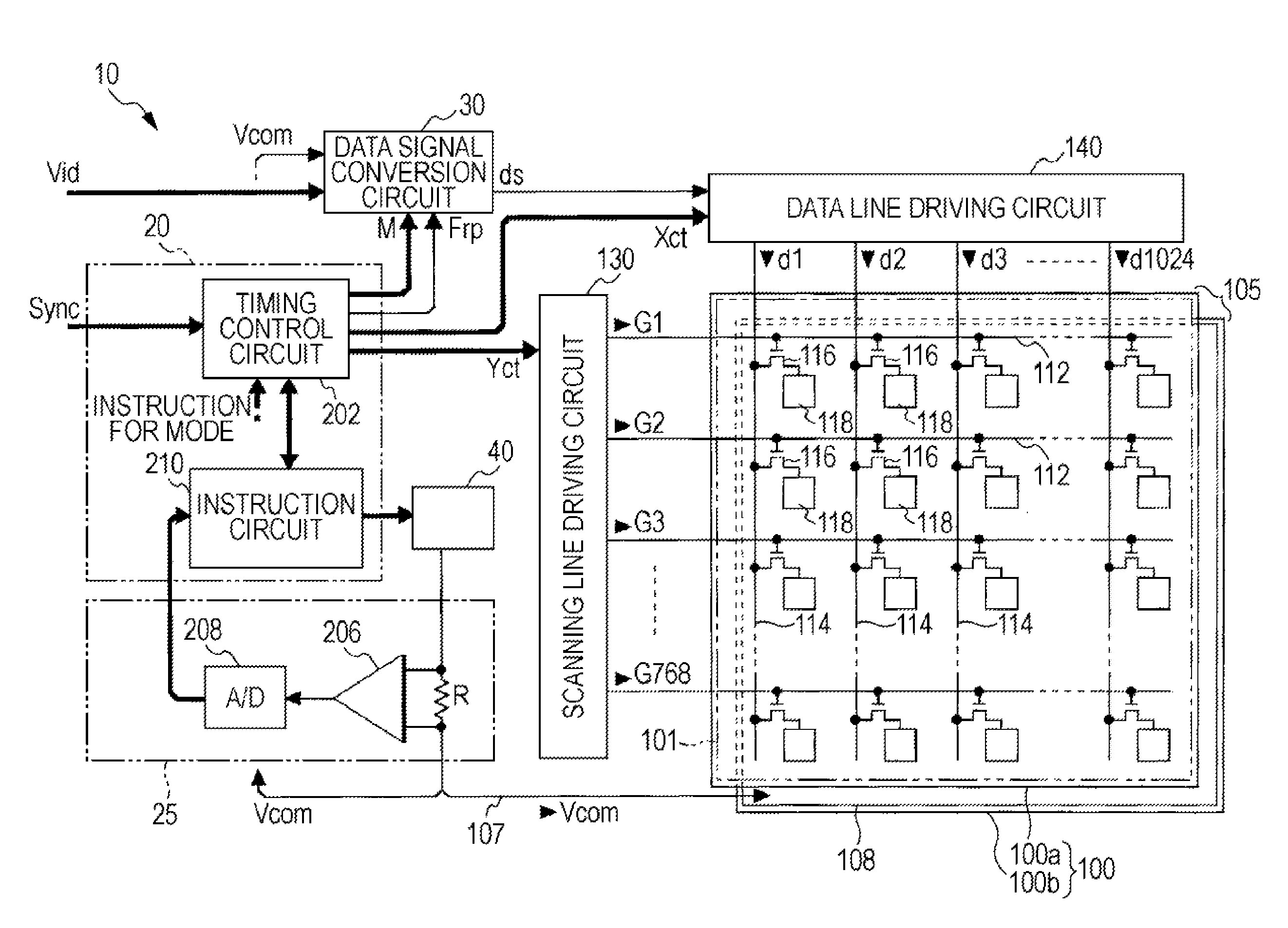
[0033]To begin with, a first embodiment of the invention will be described. FIG. 1 is a block diagram illustrating an entire configuration of a liquid crystal display (“LCD”) according to the first embodiment.
[0034]As shown in this figure, an LCD 10 includes a control circuit 20, a detection circuit 25, a data signal conversion circuit 30, a common electrode driving circuit 40, a panel assembly 100, a scanning line driving circuit 130, and a data line driving circuit 140.
[0035]The LCD 10 has two operation modes, a display mode where the panel assembly 100 performs a display operation based on a video signal Vid supplied from an external device (not shown), and a detection adjustment mode where a current zero reference value is detected and also a voltage applied to liquid crystal elements is adjusted to suppress application of a DC component to the liquid crystal layer.
[0036]The operation mode is in principle set to the display mode, but on exceptional occasions is transferred to th...
second embodiment
[0114]The first embodiment increases or decreases the common voltage Vcom so that the positive voltage effective value and the negative voltage effective value in the liquid crystal elements 120 are equal to each other. The second embodiment applies each of the positive voltage and the negative voltage once to the pixel electrodes 118 of the respective liquid crystal elements 120, twice in total for a single frame period, and also controls a rate of a duration where the positive voltage is maintained and a duration where the negative voltage is maintained.
[0115]FIG. 8 is a block diagram illustrating an entire configuration of an LCD according to a second embodiment. The LCD shown in this figure is different from one in the first embodiment in that the instruction circuit 210 instructs the timing control circuit 202, not the common electrode driving circuit 40, and also in a method that the scanning line driving circuit 130 selects the scanning lines.
[0116]Thereby, in the second embo...
third embodiment
[0132]The third embodiment of the invention will be described. The liquid crystal elements 120 used to detect the current are also used to perform a display operation in the first and second embodiments; however, the liquid crystal elements are only used for detection (i.e., detection only) in the third embodiment.
[0133]As shown in FIG. 12, in the third embodiment, a first electrode 119 with a tetragonal shape, is provided outside the display area 101 on the rear face of the element panel 100a, and a second electrode 109 is provided on the opposite panel 100b so as to face the first electrode 119.
[0134]Thereby, the liquid crystal layer 105 is sandwiched by the first electrode 119 and the second electrode 109, and this is the same as the liquid crystal elements 120 in which the liquid crystal layer 105 is sandwiched by the pixel electrodes 118 and the common electrode 108. However, the liquid crystal elements in which the liquid crystal layer 105 is sandwiched by the first electrode ...
PUM
 Abstract
Description
Claims
Application Information


