Structure and method for making a strained silicon transistor

a technology of strained silicon and strained channels, which is applied in the direction of semiconductor devices, basic electric elements, electrical appliances, etc., can solve the problems of significant challenges, relaxed crystalline silicon is said to be lattice-mismatched with respect to relaxed crystalline sige, etc., to prevent latching, block other parasitic effects, and eliminate leakage occurrence

Inactive Publication Date: 2014-05-06
STMICROELECTRONICS SRL
View PDF17 Cites 3 Cited by
  • Summary
  • Abstract
  • Description
  • Claims
  • Application Information

AI Technical Summary

Benefits of technology

[0010]The transistor is electrically isolated from a substrate to eliminate leakage occurrence, prevent latch-up, and block other parasitic effects.

Problems solved by technology

Significant challenges are faced when CMOS devices are scaled into the sub-100 nm regime.
Relaxed crystalline silicon is said to be lattice-mismatched with respect to relaxed crystalline SiGe due to the difference in their lattice constants.

Method used


Image

  • Structure and method for making a strained silicon transistor
  • Structure and method for making a strained silicon transistor
  • Structure and method for making a strained silicon transistor

Examples


Embodiment Construction

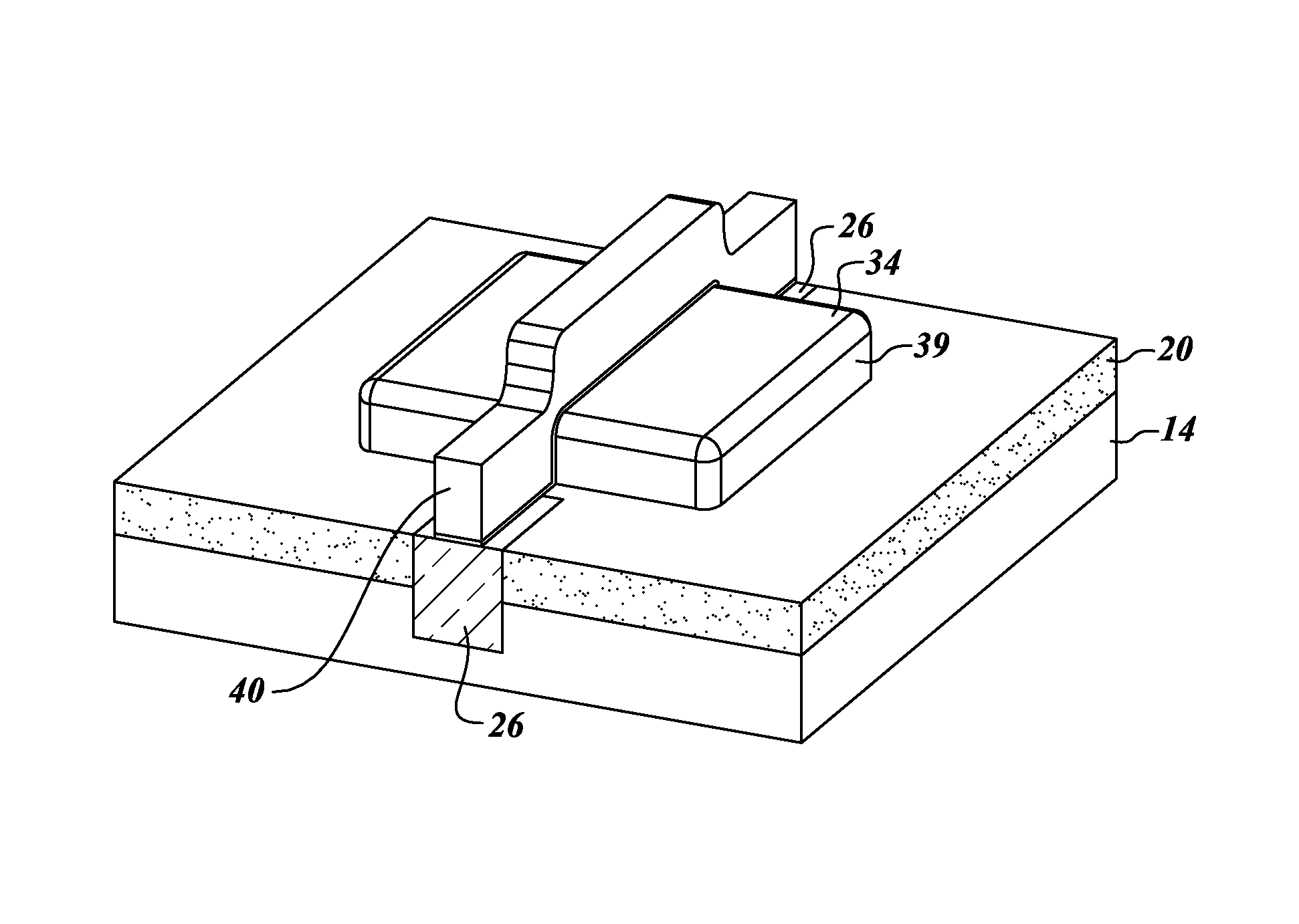
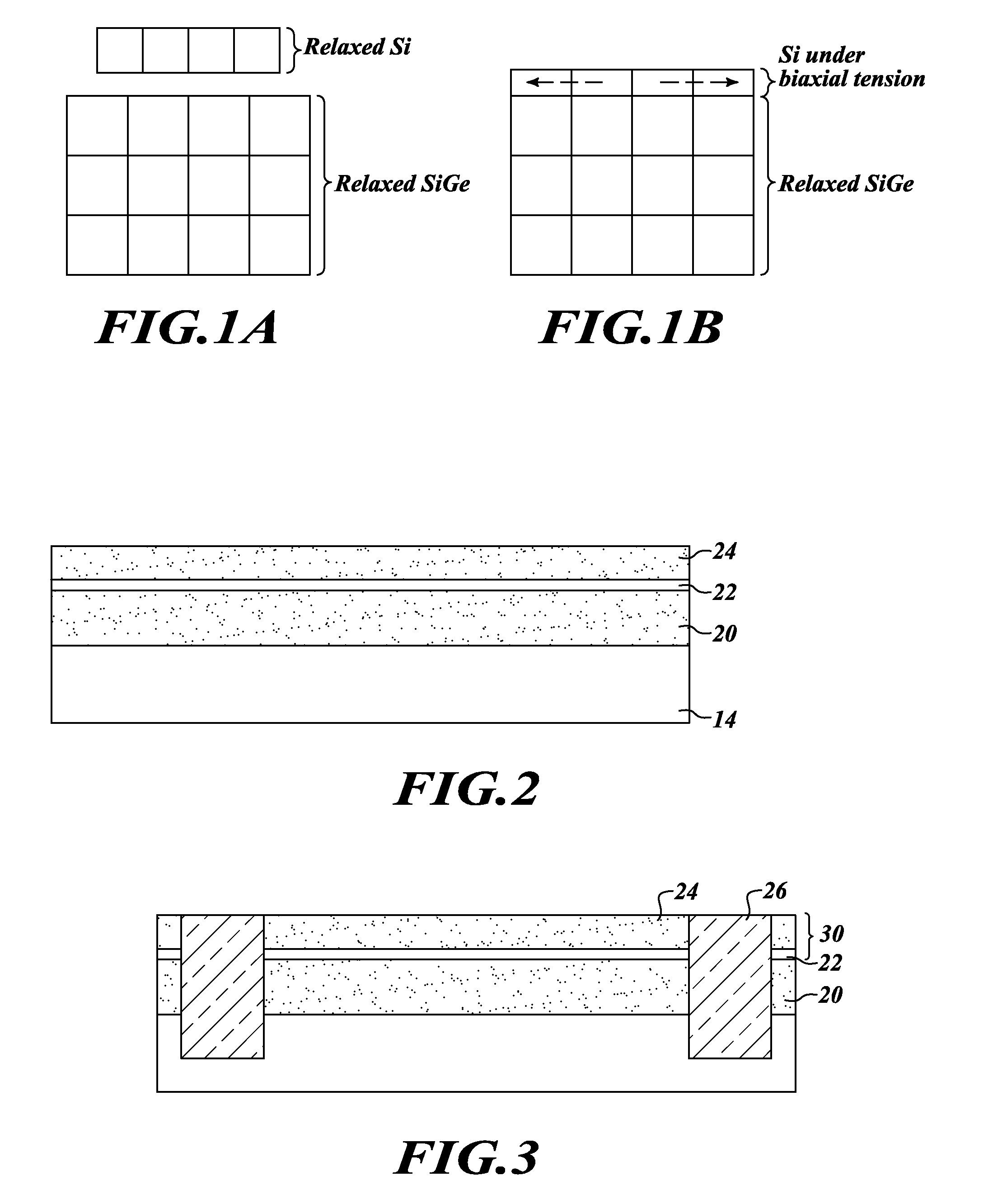
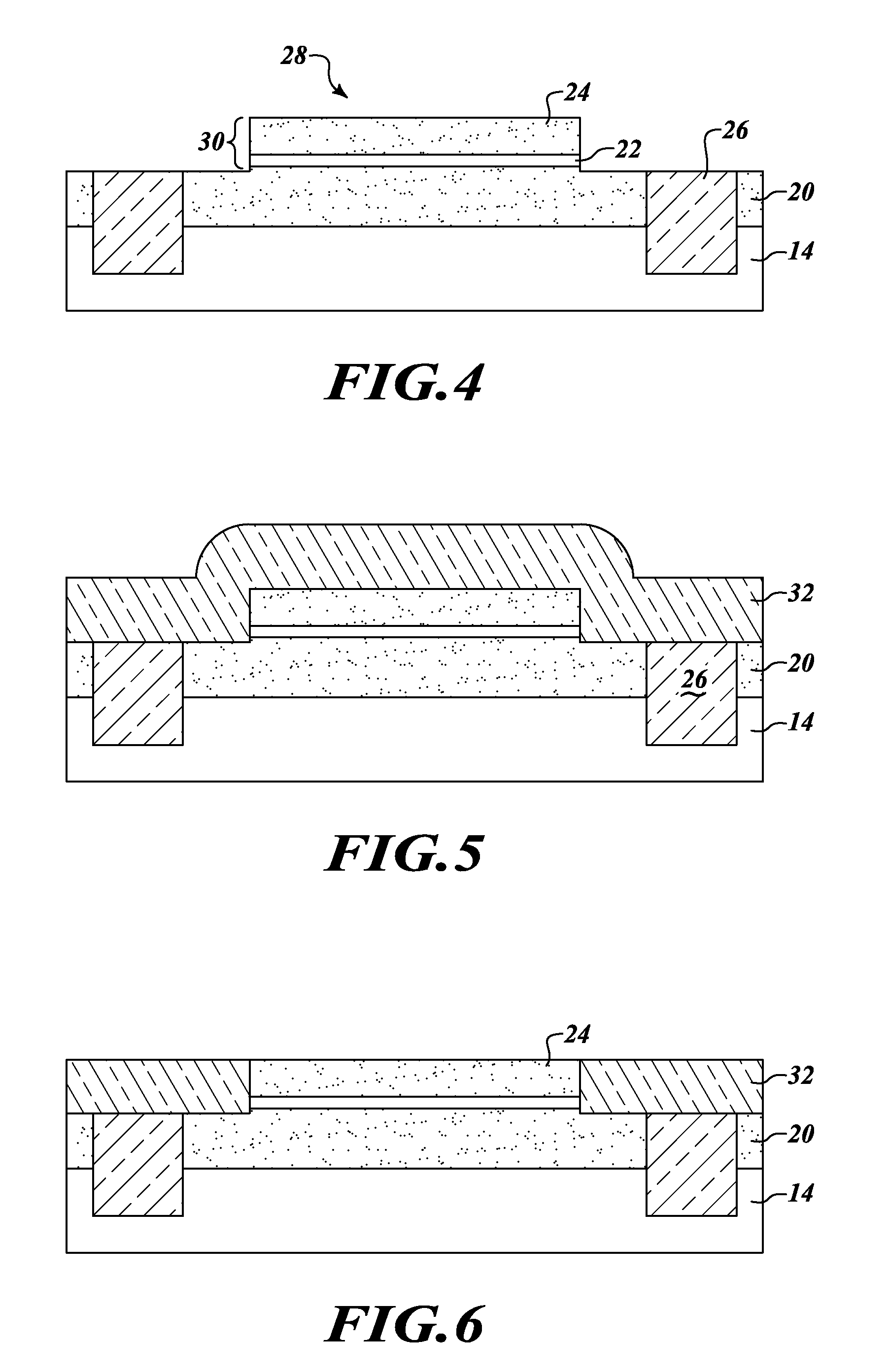
[0021]As shown in FIG. 2, a graded SiGe layer 20 is grown by an epitaxial process on top of a silicon substrate 14. The SiGe layer 20 is graded having a higher percentage of silicon adjacent the single crystalline substrate 14 and gradually reducing the percentage of silicon as it grows away from the substrate 14. A single crystal silicon layer 22 is formed overlying the graded SiGe layer 20.

[0022]The amount of lattice mismatch, and thus the amount of tension on the silicon layer 22, depends on the relative percentages of Si to Ge in the SiGe layer 20. When SiGe is formed, the percentage of each of the two elements can vary based on the formula of Si1-xGex in which x is the percentage of each of the two elements. A higher percentage of x for Si results in a lower mismatch and less stress at the junction of the silicon layer 22 and the SiGe layer 20.

[0023]Conversely, a lower percentage of Si and a higher percentage of Ge results in a greater mismatch and a higher stress. The amount o...


PUM


Abstract

A graded SiGe sacrificial layer is epitaxially grown overlying a silicon substrate. A single crystal silicon layer is then grown by an epitaxial process overlying the graded SiGe layer. A SiGe layer is next grown by an epitaxial process as a single crystal layer overlying the silicon layer. A subsequent silicon layer, which becomes the active silicon layer for the transistors, is epitaxially grown overlying the second silicon germanium layer. Together the epitaxially grown Si, SiGe and Si layers form a laminate semiconductor structure. A MOS transistor is then formed on the active area of the single crystal silicon. The graded SiGe sacrificial layer is removed by an etch process to electrically isolate the laminate semiconductor structure from the substrate.

Description

CROSS-REFERENCE TO RELATED APPLICATION[0001]This application claims the benefit under 35 U.S.C. §119(e) of U.S. Provisional Patent Application No. 61 / 286,268 filed Dec. 14, 2009. The provisional application is incorporated herein by reference in its entirety.BACKGROUND[0002]1. Technical Field[0003]This invention relates to silicon transistors, and more particularly to a silicon transistor having a strained channel.[0004]2. Description of the Related Art[0005]Complementary metal-oxide-semiconductor (CMOS) technology is a dominant semiconductor technology used for the manufacture of ultra-large scale integrated (ULSI) circuits today. Size reduction of the metal-oxide-semiconductor field-effect transistor (MOSFET) has provided significant improvement in the speed performance, circuit density, and cost per unit function of semiconductor chips over the past few decades. Significant challenges are faced when CMOS devices are scaled into the sub-100 nm regime. An attractive approach for ad...

Claims


Application Information

Patent Timeline
Patent Type & Authority Patents(United States)
IPC IPC(8): H01L21/336H01L29/772
CPCH01L29/78687H01L27/1203H01L29/66742H01L21/84H01L21/823807
Inventor DOVE, BARRY
Owner STMICROELECTRONICS SRL
Why Eureka
Try Eureka