Method of making bulk InGaN substrates and devices thereon

a technology of ingan active layers and substrates, which is applied in the direction of crystal growth process, semiconductor lasers, polycrystalline material growth, etc., can solve the problems of reducing radiative efficiency, affecting the performance of longer-wavelength devices grown on these structures, and affecting the performance of shorter-wavelength counterparts, so as to achieve a wider range of applicability

Active Publication Date: 2014-05-20
SLT TECH
View PDF267 Cites 35 Cited by
  • Summary
  • Abstract
  • Description
  • Claims
  • Application Information

AI Technical Summary

Benefits of technology

[0010]In an alternative specific embodiment, the present invention provides a method for forming a relaxed epitaxial AlxInyGa(1-x-y)N layer. The method includes providing a substrate having an orientation within about 5 degrees of a c-plane and forming at least one epitaxial AlxInyGa(1-x-y)N layer with a thickness of at least 100 nanometers such that a plurality of misfit dislocations are included to reduce a bi-axial strain within the thickness or form a relaxed state.
[0011]One or more benefits may be achieved using one or more of the specific embodiments. As an example, the present device and method provides a substantially relaxed region for device fabrication using a gallium and nitrogen containing substrate. In a specific embodiment, the present method and device can be made using conventional techniques and is cost effective. In a preferred embodiment, dislocations are introduced into a thickness of the epitaxial layer to cause relaxation that is substantially biaxial. Depending upon the embodiment, one or more of these benefits can be achieved. These and other benefits are further described throughout the present specification and more particularly below.

Problems solved by technology

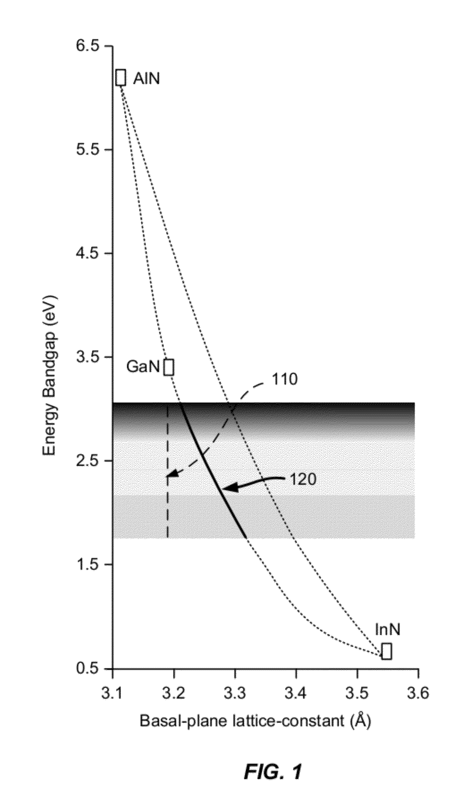
The resulting built-in stress within the InGaN active layers can be problematic for achieving high quality material and good device operation as the InN mole fraction increases, a requirement for longer wavelength devices.
For c-plane grown devices, increasing InN increases the built-in electric fields across the active layers due to spontaneous and piezoelectric polarization fields, reducing the overlap between electrons and holes and decreasing radiative efficiency.
Moreover, there is evidence for material breakdown as the stress level becomes too high, resulting in so-called “phase separation,” beyond a critical limit of a certain InN mole fraction combined with a certain layer thickness.
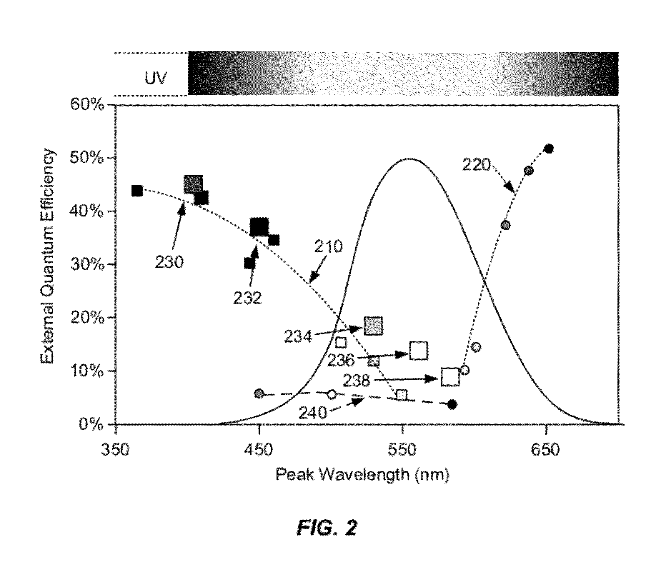
The performance of longer-wavelength devices grown on these structures, however, still suffers considerably compared to that of shorter-wavelength counterparts.

Method used


Image

  • Method of making bulk InGaN substrates and devices thereon
  • Method of making bulk InGaN substrates and devices thereon
  • Method of making bulk InGaN substrates and devices thereon

Examples


Embodiment Construction

[0022]According to the present invention, techniques related generally to using bulk gallium and nitrogen containing substrates are provided. More particularly, the present invention provides a method and device using bulk gallium and nitrogen containing substrates configured in a semi-polar orientation. Merely by way of example, the invention has been applied to use bulk GaN substrates to form overlying epitaxial regions in a bi-axially relaxed state, but it would be recognized that the invention has a broader range of applicability.

[0023]FIG. 3 is a diagram of an epitaxial layer 303 on a substrate 301. In one embodiment, substrate 301 comprises bulk GaN. In other embodiments, substrate 301 comprises AlN, sapphire, silicon carbide, gallium arsenide, MgAl2O4 spinel, ZnO, BP, ScAlMgO4, YFeZnO4, MgO, Fe2NiO4, LiGa5O8, Na2MoO4, Na2WO4, In2CdO4, LiAlO2, LiGaO2, Ca8La2(PO4)6O2, or the like. Preferably, substrate 301 comprises bulk GaN with a surface dislocation density below about 107 cm...


PUM


Abstract

A relaxed epitaxial AlxInyGa(1-x-y)N layer on a substrate having a semipolar surface orientation includes a plurality of misfit dislocations in portions of the thickness of the epitaxial layer to reduce bi-axial strain to a relaxed state.

Description

CROSS-REFERENCES TO RELATED APPLICATIONS[0001]This Non-Provisional patent application is based on and claims priority to Provisional Patent Application No. 61 / 392,565, titled METHOD OF MAKING BULK InGaN SUBSTRATES AND DEVICES THEREON, filed on Oct. 13, 2010. This provisional application is incorporated herein by reference for all purposes.BACKGROUND OF THE INVENTION[0002]The present invention relates generally to techniques using bulk gallium and nitrogen containing substrates. More particularly, the present invention provides a method and device using bulk gallium and nitrogen containing substrates configured in a semi-polar orientation. Merely by way of example, the invention has been applied to use bulk GaN substrates to form overlying epitaxial regions in a bi-axially relaxed state, but it would be recognized that the invention has a broader range of applicability.[0003]Today's state-of-the-art visible-spectrum light-emitting diodes (LEDs) and laser diodes (LDs) in the ultraviol...

Claims


Application Information

Patent Timeline
Patent Type & Authority Patents(United States)
IPC IPC(8): H01L29/15H01L33/00H01L29/06H01L21/31
CPCH01L21/0265H01L33/32H01L21/02389H01S5/32341H01L21/0254H01S5/0206C30B25/186H01L21/02639H01L33/20H01L33/0075C30B29/406H01L21/02458H01L21/02433H01L33/12H01L21/0251H01L33/16H01L21/0237
Inventor KRAMES, MIKED'EVELYN, MARKPAKALAPATI, RAJEEVALEXANDER, ALEXKAMBER, DERRICK
Owner SLT TECH
Why Eureka
Try Eureka