Grinding/electrolysis combined multi-wire-slicing processing method for silicon wafers

a processing method and electrolysis technology, applied in electrolysis components, electrical-based machining electrodes, manufacturing tools, etc., can solve the problems of increasing the slicing thickness of silicon wafers, reducing the processing efficiency of silicon wafers, and not considering the residue of metal elements on the surface of silicon wafers. , to achieve the effect of easy transplantation

Inactive Publication Date: 2014-06-10
NANJING UNIV OF AERONAUTICS & ASTRONAUTICS
View PDF9 Cites 2 Cited by
  • Summary
  • Abstract
  • Description
  • Claims
  • Application Information

AI Technical Summary

Benefits of technology

[0019]1. Electrolysis is favorable to reduce mechanical cutting force. The slicing product plays a role of abrasive and may lower the probability of wire fracture and improve the slicing efficiency of silicon wafers.
[0020]2. Mechanical grinding effect makes for the continuity of electrochemical passivation (or corrosion), makes the mechanically damaged layers of the silicon wafers thinner and the surface more integral, reduces follow-up thickness reduction and improves the material utilization.
[0021]3. Thinner slicing wires and less (or thin) abrasive may be used, thereby reducing the thickness of silicon wafers and the width of the kerf and further improving the material utilization. Particularly to the silicon wafers of above 200 mm, the width of the kerf and the thickness of the silicon wafers may both be smaller than 150 μm, thereby breaking through the limit of conventional multi-wire-slicing process.
[0022]4. It provides a new technological approach for the development of MWS devices and may be easily transplanted to the existing or being researched and developed MWS devices.

Problems solved by technology

Currently thin silicon wafers with a large area (30 cm×30 cm) can be produced by MWS method, but as it is non-rigid slicing, inevitably the metal slicing wires are deformed and consequently generate instantaneous impact on the cut silicon wafers continuously in the slicing process.
Technically speaking, it is rather difficult to further reduce the thickness of existing large-size silicon wafers, increase the slicing thickness of silicon wafers, control slicing loss and realize cost-effective and efficient slicing.
Nonetheless, in the foregoing relevant research, deionized water is used as the working medium, so the discharge energy is large and there is obvious heat affected zones on the surface of the silicon wafers and the processing efficiency is not high (at present, the highest slicing efficiency 2 / min).
Furthermore, the residue of metal elements on the surface of the silicon wafers is not considered.
For this reason, it still can not compatible with solar energy silicon wafer cell manufacturing process.
However, during MWS of silicon wafers, the discharge current is too large and wires are prone to breaking.
As a result, this method can not be applied in MWS technology.

Method used


Image

  • Grinding/electrolysis combined multi-wire-slicing processing method for silicon wafers
  • Grinding/electrolysis combined multi-wire-slicing processing method for silicon wafers

Examples


embodiment 1

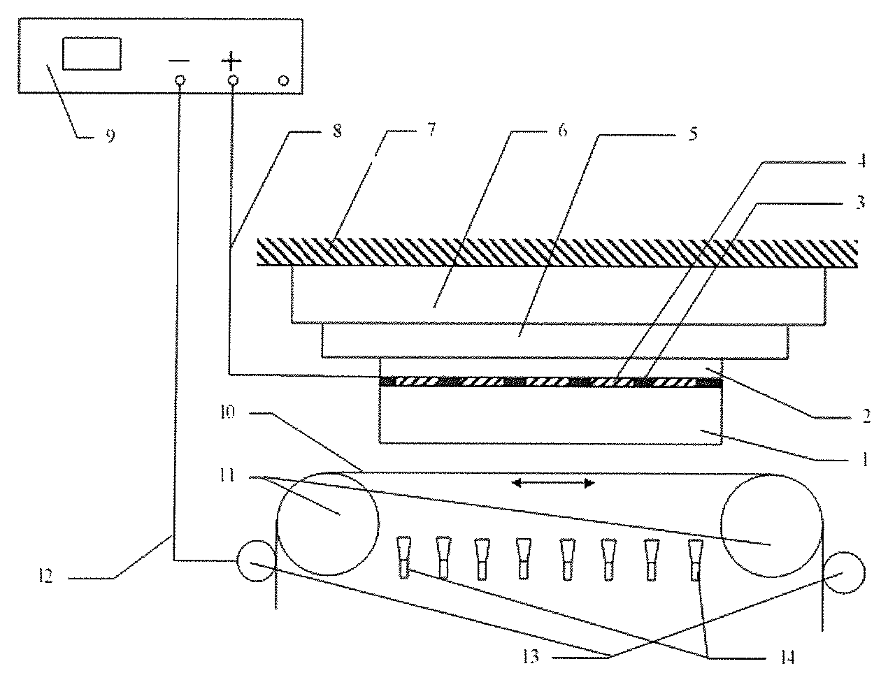
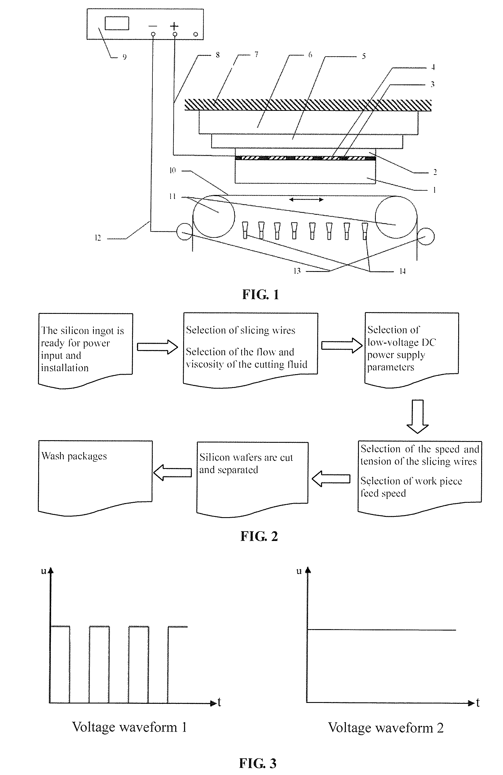
[0030]A grinding / electrolysis combined multi-wire-slicing processing method for solar energy silicon wafers, comprising the following steps:

[0031]① A solar energy silicon rod (ingot) is mounted onto the workbench of a multi-wire slicing machine tool. This workbench has a mechanism controlling lifting motion. The feed speed is 0.1˜2 mm / min;

[0032]② The copper plating alloy steel wire and the silicon rod (or silicon ingot) are externally connected to a low-voltage continuous (or impulse) DC power supply. The voltage amplitude is adjustable in the range of 0˜30V and the duty cycle is adjustable in the range of 0˜10 as long as the requirements of anode passivation (or corrosion) are met. The selection of a continuous (or impulse) working mode may control the electrochemical effect;

[0033]The copper plating alloy steel wire is connected to the cathode of the power supply by adding power input devices at the locations where the copper plating alloy steel wire enters and leaves the slicing z...

embodiment 2

[0053]A grinding / electrolysis combined multi-wire-slicing processing method for solar energy silicon wafers, comprising the following steps:

[0054]① A solar energy silicon rod (or silicon ingot) is mounted onto the workbench of a multi-wire slicing machine tool. This workbench has a mechanism controlling lifting motion. The feed speed is 0.1˜2 mm / min;

[0055]② The diamond fixed abrasive spring steel wire and the silicon ingot (or silicon rod) are externally connected to a continuous (or impulse) low-voltage DC power supply. The voltage amplitude is adjustable in the range of 0˜30V and the duty cycle is adjustable in the range of 0˜10 as long as the requirements of anode passivation (or corrosion) are met. The selection of a continuous (or impulse) working mode may control the electrochemical effect;

[0056]The diamond fixed abrasive spring steel wire is connected to the cathode of the power supply by adding power input devices at the locations where the diamond fixed abrasive spring stee...


PUM

PropertyMeasurementUnit
diameteraaaaaaaaaa
voltage amplitudeaaaaaaaaaa

Abstract

A grinding / electrolysis combined multi-wire-slicing processing method for silicon wafers includes the following steps: first, with a metal slicing wire (10) provided on a multi-wire-slicing machine serving as cathode, a silicon rod or a silicon ingot (1) (anode) is processed by grinding / electrolysis combined multi-wire-slicing through application of a voltage; second, during said processing, the metal slicing wire (10) and the silicon rod or a silicon ingot (1) are connected with a low-voltage continuous or pulsed direct current power supply (9); third, an electrolytic liquid is sprayed into the cutting area to ensure cooling and anode erosion. The method reduces macroscopic cutting force and enables a grinding / electrolysis combined multi-wire-slicing processing method for large size ultra-thin silicon wafers.

Description

CROSS-REFERENCE TO RELATED APPLICATION(S)[0001]This application is a National Phase Patent Application and claims priority to and benefit of International Application Number PCT / CN2010 / 075147, filed on Jul. 14, 2010, which claims priority to and benefit of Chinese Patent Application Number 201010141727.3, filed on Apr. 8, 2010, the entire disclosure of which are incorporated herein by this reference.FIELD OF THE INVENTION[0002]The present invention relates to a method for cutting silicon wafers by using grinding / electrolysis combined processing technology, specifically to a grinding electrolysis combined multi-wire-slicing processing for silicon wafers. This method is also applicable to the grinding electrolysis combined multi-wire-slicing processing of semiconductor materials.BACKGROUND OF THE INVENTION[0003]Silicon wafer is a main production raw material on semiconductor and photovoltaic industrial chains. MWS (Multi-Wire-Slicing) is a process for cutting brittle and hard material...

Claims


Application Information

Patent Timeline
Patent Type & Authority Patents(United States)
IPC IPC(8): B23H7/08B23H5/08H01L21/02B23H1/00B23H5/10B23H7/02B23H5/00B23H5/06
CPCB23H7/02B23H5/06H01L21/02B23H5/08B23H5/10B23H7/08B23H5/00B23H9/00B23H1/00H01L21/02002
Inventor WANG, WEILIU, ZHENGXUN
Owner NANJING UNIV OF AERONAUTICS & ASTRONAUTICS
Why Eureka
Try Eureka