Method for forming interlayer connectors to a stack of conductive layers

a technology of interlayer connectors and conductive layers, which is applied in the direction of basic electric elements, semiconductor devices, electrical equipment, etc., can solve the problems of increasing the cost of interconnection implementation with the number of lithographic steps, and using separate masks. achieve the effect of increasing the size of the open etch region

Active Publication Date: 2014-06-24
MACRONIX INT CO LTD
View PDF3 Cites 37 Cited by
  • Summary
  • Abstract
  • Description
  • Claims
  • Application Information

AI Technical Summary

Benefits of technology

[0011]A first example of a method, for use with an electronic device including a stack comprising a plurality of conductive layers interleaved with a plurality of dielectric layers, for forming interlayer connectors extending to respective ones of the plurality of conductive layers is carried out as follows. Portions of the conductive layers and the dielectric layers in the stack are removed to form landing areas on the plurality of conductive layers in the stack. The landing areas are without overlying conductive layers in the stack, and W is the number of conductive layers. The removing step comprises the following. The stack of dielectric / conductive layers is etched to expose landing areas at W−1 conductive layers using a set of M etch masks. The etch masks have mask regions and spaced apart open etch regions. M is greater than or equal to 2, and NM as less than or equal to W. N is an integer greater than or equal to 3. For each etch mask m in the set, where m goes from 0 to M−1, perform the following. (a) Form etch mask m over the contact region, the etch mask having open etch regions over some of the landing areas. (b) Etch through Nm conductive layers at the open etch regions of mask m. (c) Trim etch mask m to increase the size of the open etch regions to overlie additional contact openings. (d) Etch Nm conductive layers at the increased size open etch regions. (g) If N is greater than 3, repeat the (c) trim step and the (d) etch step N−3 times. Whereby the landing areas on the plurality of conductive layers are exposed with different combinations of the etch masks.

Problems solved by technology

The cost to implement the interconnections increases with the number of lithographic steps needed.
However, one of the drawbacks with conventional 3-D stacked memory devices is that a separate mask is typically used for each contact level.

Method used


Image

  • Method for forming interlayer connectors to a stack of conductive layers
  • Method for forming interlayer connectors to a stack of conductive layers
  • Method for forming interlayer connectors to a stack of conductive layers

Examples


Embodiment Construction

[0032]The following description will typically be with reference to specific structural embodiments and methods. It is to be understood that there is no intention to limit the invention to the specifically disclosed embodiments and methods but that the invention may be practiced using other features, elements, methods and embodiments. Preferred embodiments are described to illustrate the present invention, not to limit its scope, which is defined by the claims. Those of ordinary skill in the art will recognize a variety of equivalent variations on the description that follows. Like elements in various embodiments are commonly referred to with like reference numerals.

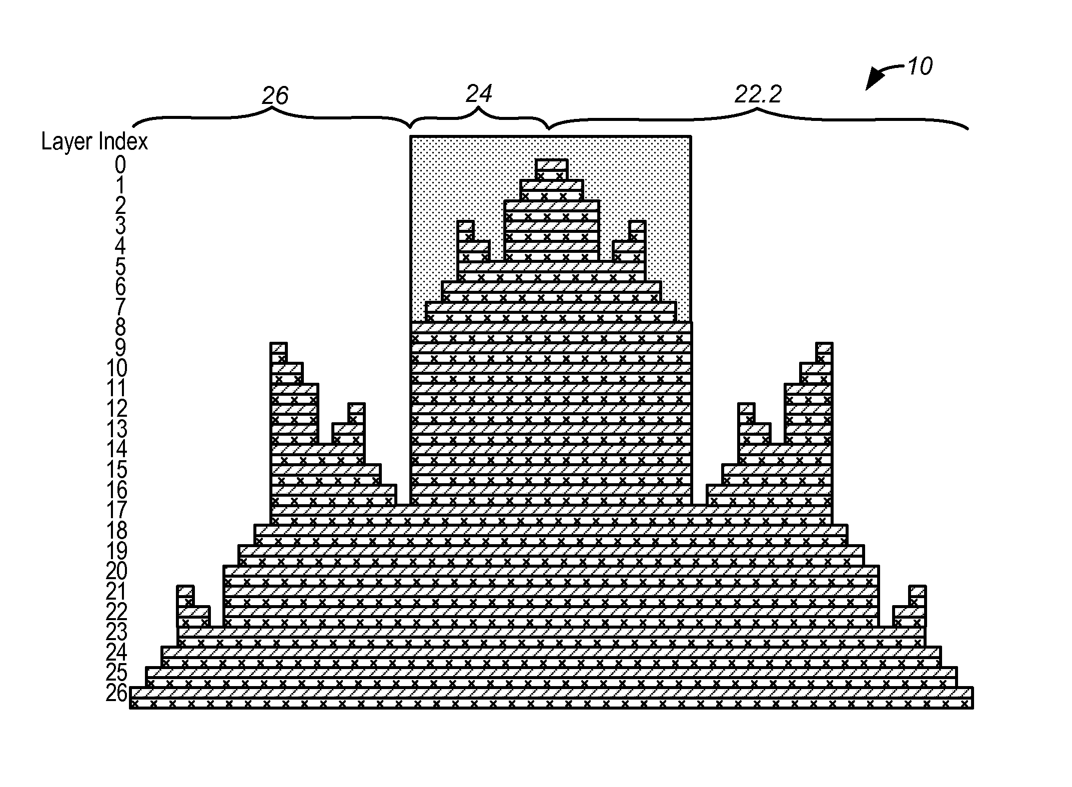
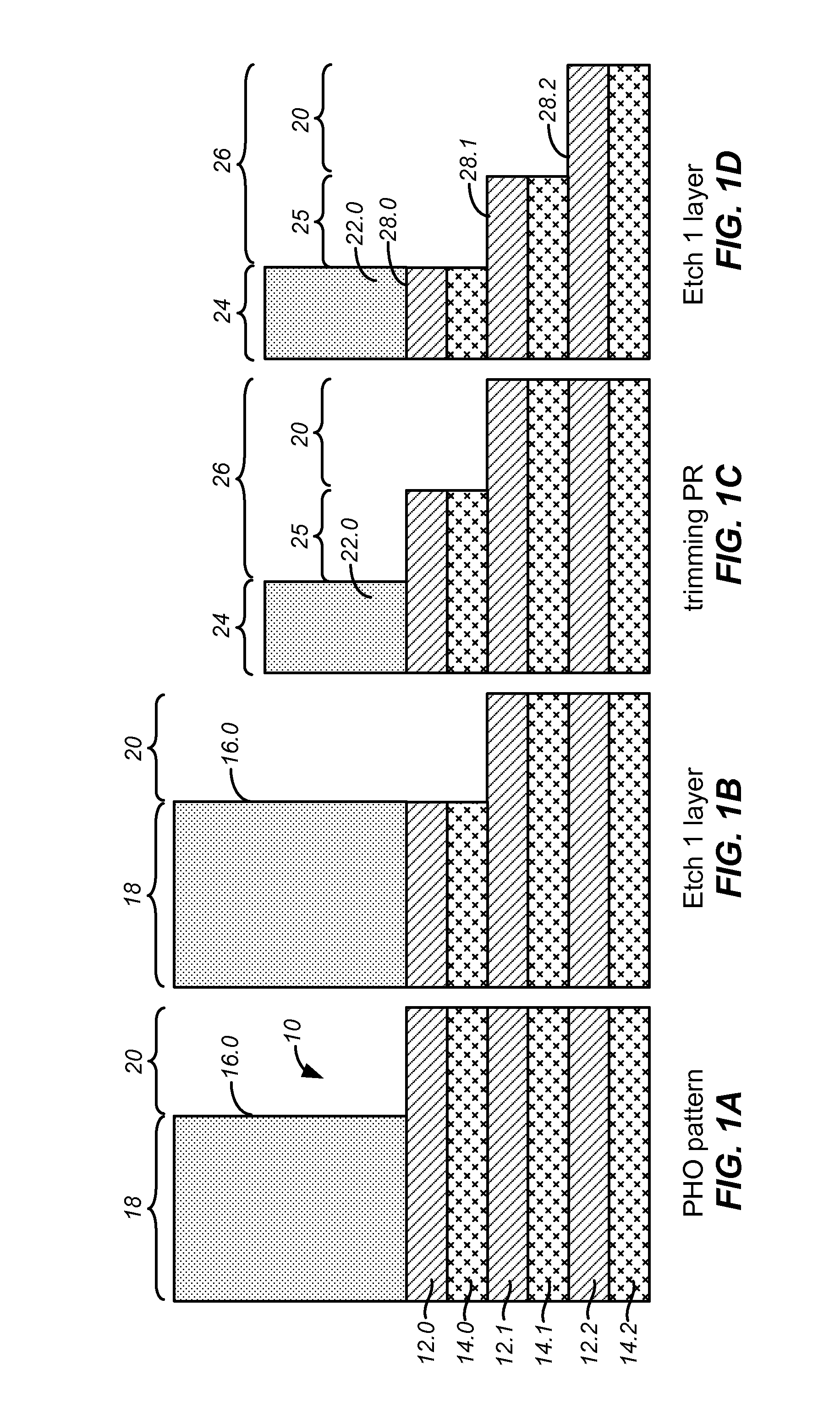
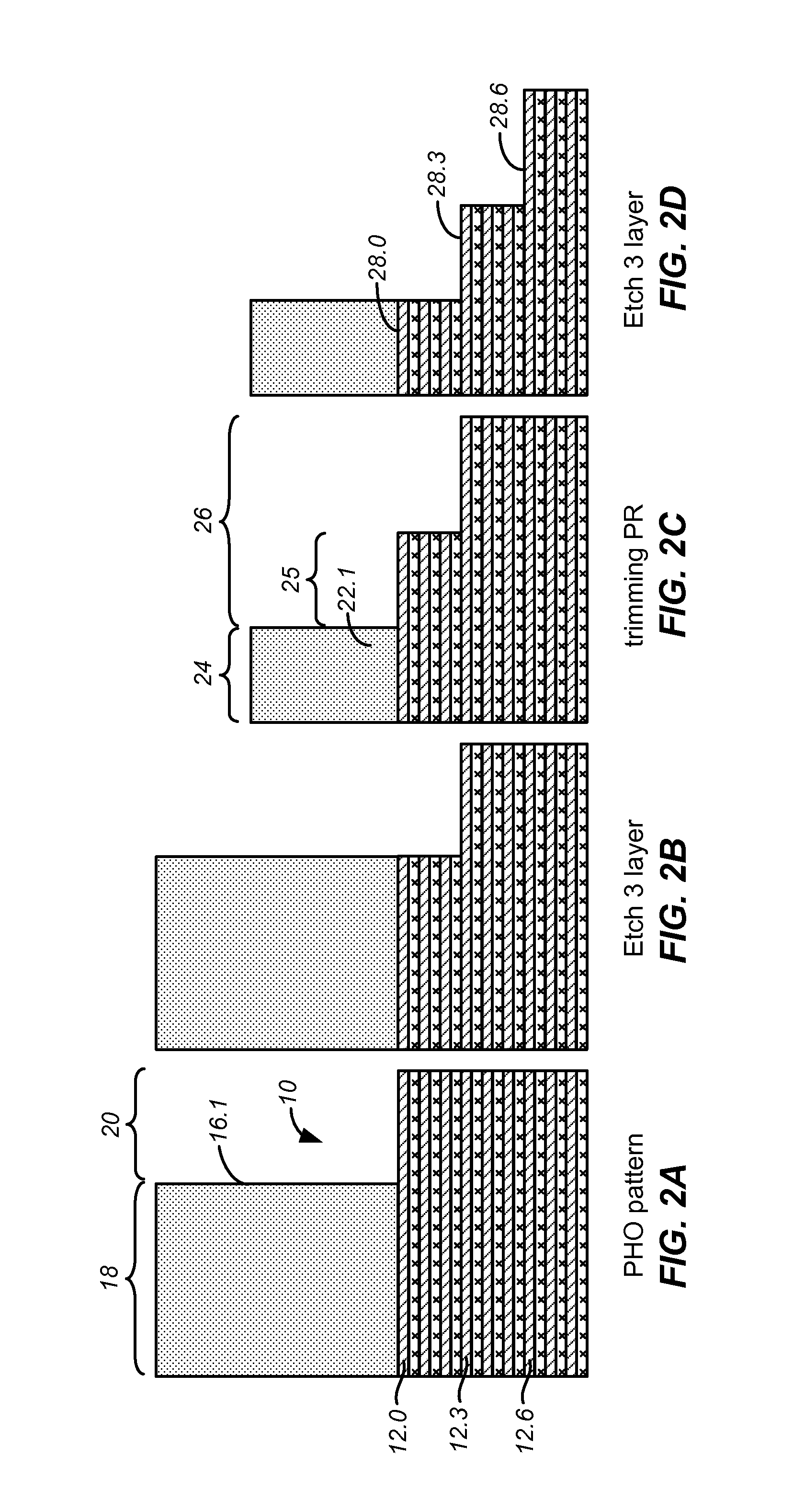
[0033]US Patent Publications US-2012-0184097-A1 and US-2012-0181701-A1 disclose what can be referred to as binary systems for forming interlayer connectors extending to the conductive layers of a stack of conductive layers interleaved with dielectric layers. In the binary system, M etch masks can be used in the creation ...


PUM


Abstract

A method forms interlayer connectors extending to conductive layers of a stack of W conductive layers interleaved with dielectric layers. The stack is etched to expose landing areas at W−1 conductive layers using a set of M etch masks. For each etch mask m, m going from 0 to M−1, there is a first etching step, at least one mask trimming step, and a subsequent etching step following each trimming step. The etch mask may cover Nm+1 of the landing areas and the open etch region may cover Nm of the landing areas. N equals 2 plus the number of trimming steps. The trimming step may be carried out so that the increased size open etch region overlies an additional 1/N of the landing areas. Part of the stack surface may be shielded during the removing step to create dummy areas without contact openings.

Description

CROSS-REFERENCE TO RELATED APPLICATIONS[0001]This application is related to the following U.S. patent applications: U.S. patent application Ser. No. 13 / 049,303, now U.S. Patent Publication No. US-2012-0184097-A1, published 19 Jul. 2012, entitled REDUCED NUMBER OF MASK FOR IC DEVICE WITH STACKED CONTACT LEVELS; U.S. patent application Ser. No. 13 / 114,931, now U.S. Patent Publication No. US-2012-0181701-A1, published 19 Jul. 2012, entitled MULTILAYER CONNECTION STRUCTURE AND MAKING METHOD; U.S. patent application Ser. No. 13 / 451,411, filed 19 Apr. 2012, entitled METHOD FOR CREATING A 3D STACKED MULTICHIP MODULE; and U.S. patent application Ser. No. 13 / 451,428, filed 19 Apr. 2012, entitled INTEGRATED CIRCUIT CAPACITOR AND METHOD; U.S. patent application Ser. No. 13 / 607,555, filed 7 Sep. 2012, entitled METHOD FOR FORMING INTERLAYER CONNECTORS IN A THREE-DIMENSIONAL STACKED IC DEVICE; and U.S. patent application Ser. No. 13 / 593,328, filed 23 Aug. 2012, entitled MULTI-LEVEL VERTICAL PLUG ...

Claims


Application Information

Patent Timeline
Patent Type & Authority Patents(United States)
IPC IPC(8): H01L21/00
CPCH01L21/76816H01L21/76838H01L27/11548H01L21/32139H01L21/0273H01L27/11575H10B41/50H10B43/50
Inventor CHEN, SHIH-HUNG
Owner MACRONIX INT CO LTD
Why Eureka
Try Eureka