

NAND flash biasing operation
a biasing operation and flash memory technology, applied in the field of flash memory technology, can solve problems such as unwanted charge tunneling into cells, reducing, and arising from charge retention
- Summary
- Abstract
- Description
- Claims
- Application Information
AI Technical Summary
Benefits of technology
Problems solved by technology
Method used
Image

Examples
Embodiment Construction
[0034]A detailed description of embodiments of the present invention is provided with reference to FIGS. 1-14.
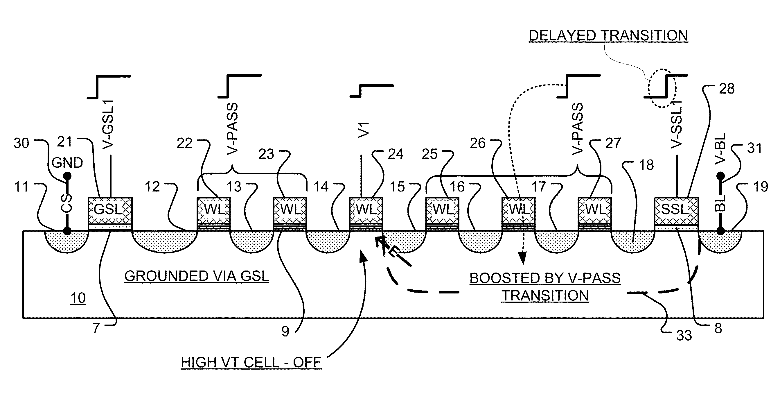
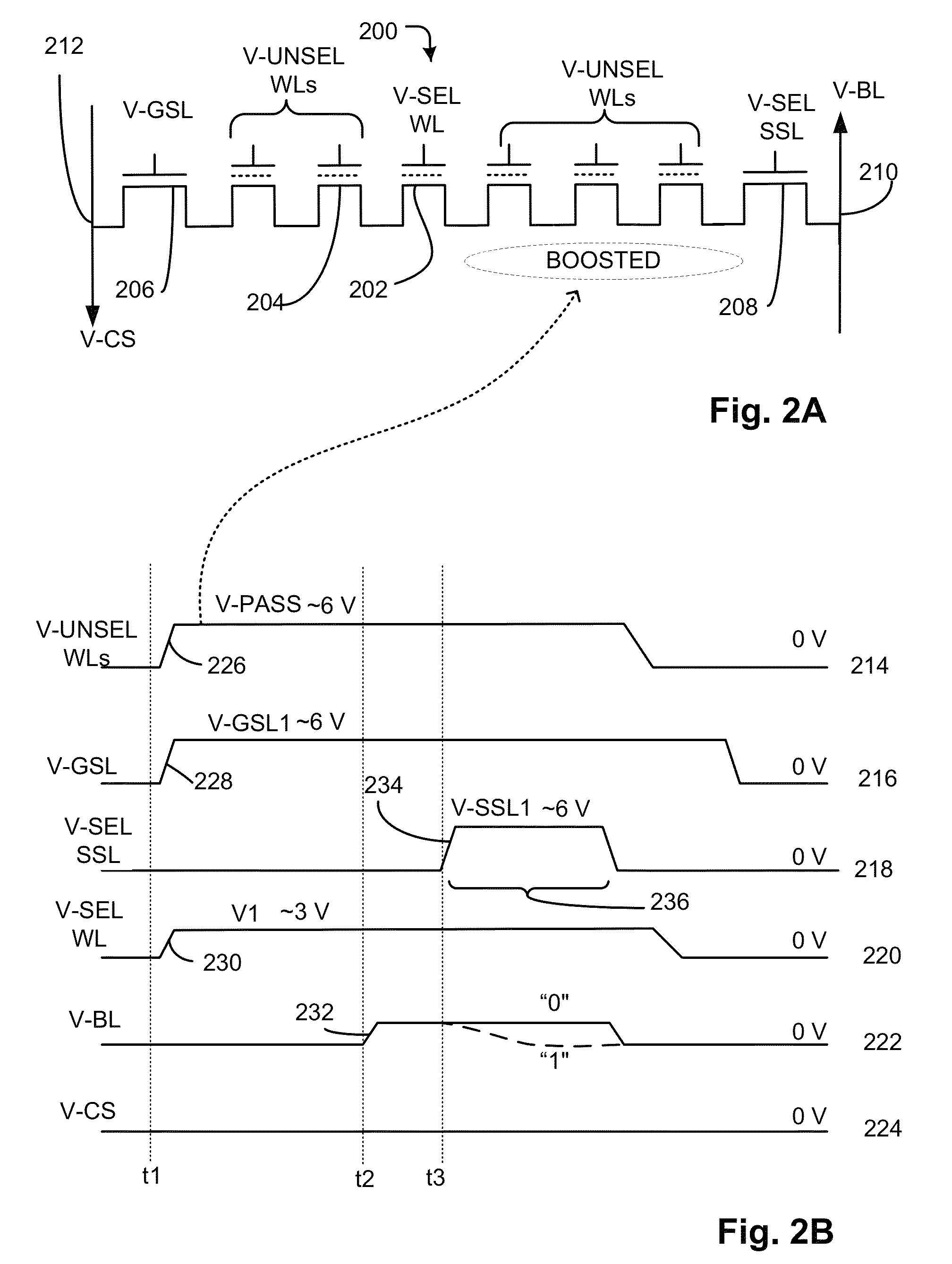
[0035]FIG. 1 is a simplified cross-sectional view of a selected NAND string that shows a bias arrangement. The NAND string includes a plurality of flash memory cells that are arranged in series. Another technology for implementation of NAND flash using bandgap engineered SONOS (BE-SONOS) charge trapping technology is described in U.S. Pat. No. 7,315,474 by Lue, which is incorporated by reference as if fully set forth herein. NAND strings can be implemented in a variety of configurations, including finFET technology, shallow trench isolation technology, vertical NAND technology and others. Yet another 3D NAND architecture is described in co-pending U.S. patent application Ser. No. 13 / 239,760 (now U.S. Patent Publication No. 2012-0182802) entitled “Memory Architecture of 3D Array With Improved Uniformity of Bit Line Capacitances” which application is incorporated by reference ...
PUM
 Abstract
Description
Claims
Application Information