Supercharge Your Innovation With Domain-Expert AI Agents!

Packing structure for a thin display device

a display device and packaging technology, applied in the direction of packaging goods, transportation and packaging, tray containers, etc., can solve the problems of display panel damage, display panel dropping off the device, image quality degradation,

Active Publication Date: 2014-07-15
PANASONIC CORP
View PDF9 Cites 4 Cited by
  • Summary
  • Abstract
  • Description
  • Claims
  • Application Information

AI Technical Summary

Benefits of technology

The packing structure effectively reduces deformation and damage to the display panels by distributing impact forces through a step-wise contact with shock-absorbing surfaces, preventing panel dislodgment and maintaining image quality during transportation.

Problems solved by technology

As the thin display devices become thinner and have narrower frames, the strength of the products decreases, which may cause deformation of display modules or cabinets, damages to the display panels, degrading of image quality as a result of drop impact, vibration or the like suffered during transportation of the packing.
Consequently, a phenomenon where the external force such as a drop impact, vibration or the like cause the display panels to be dropped off the device have become noticeable.
As described above, the external force such as a drop impact, vibration or the like suffered during transportation may cause deformation of display modules or cabinets, damages to the display panels, degrading of image quality or the like.

Method used


Image

  • Packing structure for a thin display device
  • Packing structure for a thin display device
  • Packing structure for a thin display device

Examples


Embodiment Construction

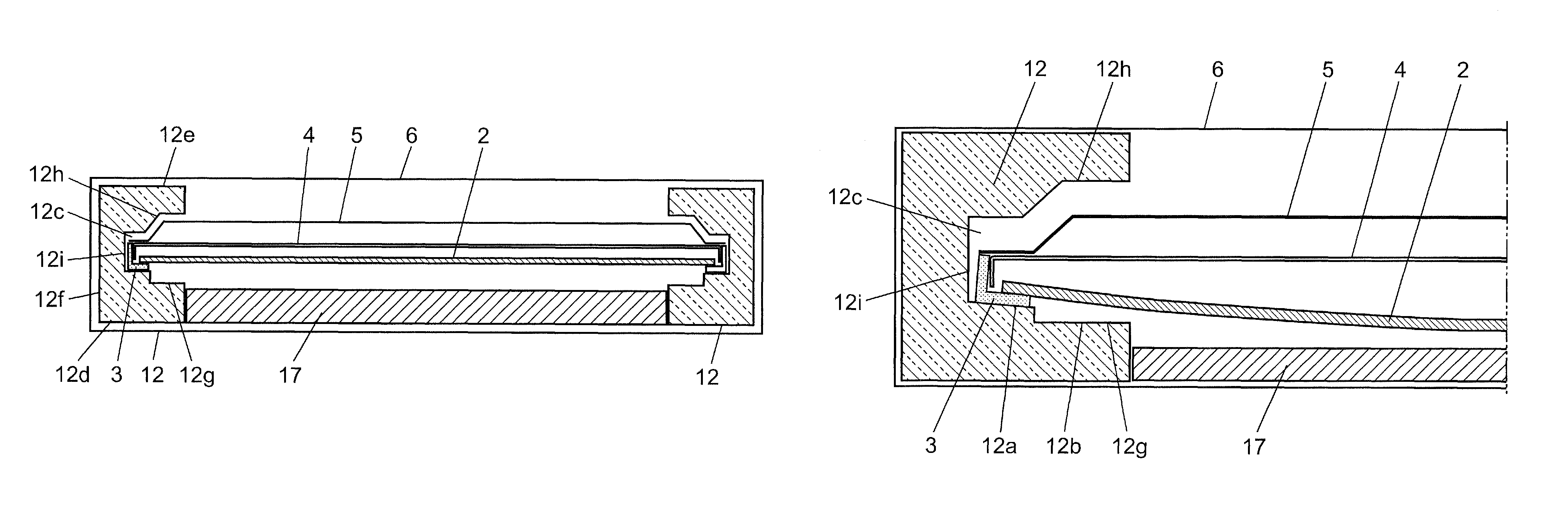
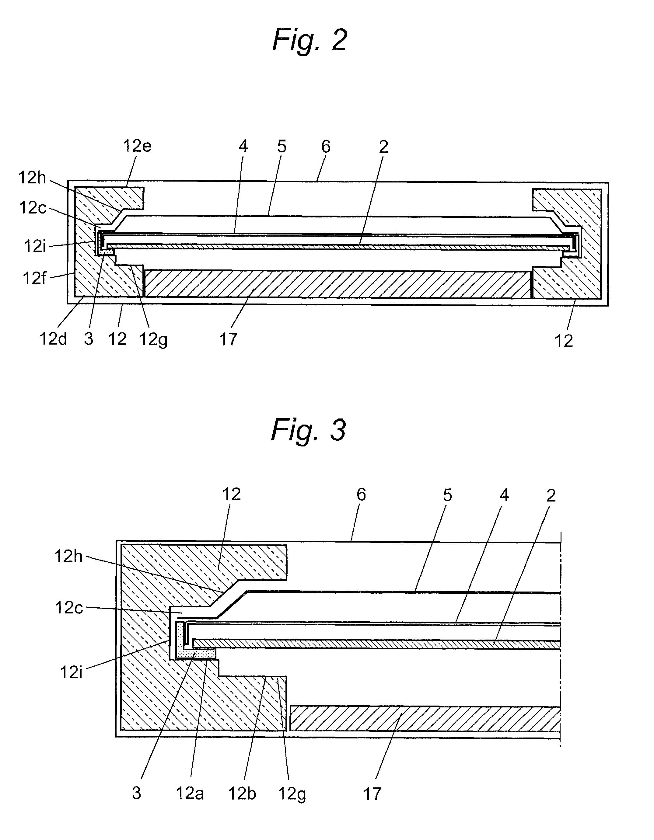
[0020]A packing structure for a liquid crystal display device according to an embodiment of the present disclosure will be described below with reference to the drawings by taking an example of a liquid crystal display device. However, unnecessarily detailed description may be omitted. For example, detailed description of already well-known matters and redundant description of substantially the same configuration may be omitted. All of such omissions are intended to facilitate understanding by those skilled in the art by preventing the following description from becoming unnecessarily redundant. The inventors provide the attached drawings and the following description for those skilled in the art to fully understand the present disclosure and do not intend to limit the subject described in the claims by the attached drawings and the following description.

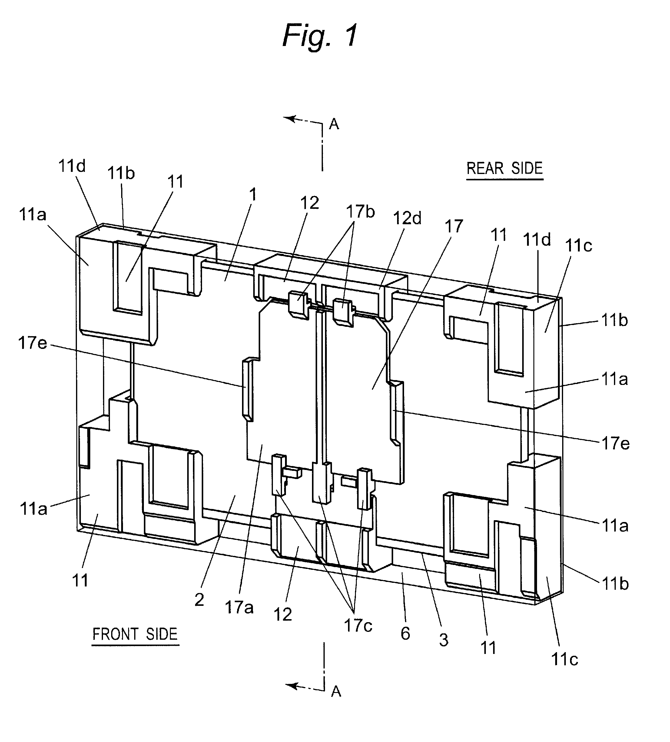
[0021]FIG. 1 is a general view showing a packing structure for liquid crystal display device 1 according to the embodiment of the ...


PUM


Abstract

A packing structure for a liquid crystal display device includes a packing box for storing the liquid crystal display device and shock-absorbing members. The shock-absorbing members are stored in the packing box together with the liquid crystal display device so as to be interposed between the liquid crystal display device and the packing box. A side wall of a groove of the shock-absorbing member has a plurality of shock-absorbing surfaces with the gap with the display panel larger in the inside of the display panel than in the outside of the display panel. A central shock-absorbing member is disposed on the inside of the display panel deeper than the shock-absorbing face. The gap between the central shock-absorbing member and the display panel is larger than that between the shock-absorbing face and the display panel.

Description

CROSS-REFERENCE TO RELATED APPLICATIONS[0001]This is a continuation application of International Application No. PCT / JP2012 / 007279, with an international filing date of Nov. 13, 2012, which claims priority of Japanese Patent Application No.: 2011-248327 filed on Nov. 14, 2011, the content of which is incorporated herein by reference.BACKGROUND[0002]1. Technical Field[0003]The present invention relates to a packing structure for a thin display device such as a liquid crystal display device and a plasma display device used as a television receiver, a monitor device or the like.[0004]2. Description of Related Art[0005]Needs for liquid crystal display devices has been growing for use as a professional as well as a residential flat-type video display unit.[0006]Generally, the packing structure for thin display device includes a liquid crystal display device, a packing box to store the liquid crystal display device, and a shock-absorbing member disposed between the liquid crystal display ...

Claims


Application Information

Patent Timeline
Patent Type & Authority Patents(United States)
IPC IPC(8): B65D85/48B65D81/05
CPCB65D85/48B65D81/053B65D81/113
Inventor NAKASE, KIYOTAKA
Owner PANASONIC CORP
Features
  • R&D
  • Intellectual Property
  • Life Sciences
  • Materials
  • Tech Scout
  • Unparalleled Data Quality
  • Higher Quality Content
  • 60% Fewer Hallucinations
Learn More