Eureka AIR delivers breakthrough ideas for toughest innovation challenges, trusted by R&D personnel around the world.

Semiconductor memory device including mode register set and method for operating the same

a memory device and mode register technology, applied in the direction of information storage, static storage, digital storage, etc., can solve the problems of increasing the size of the semiconductor memory device, reducing the cell capacity, and reducing the design efficiency, so as to reduce the time taken for generating an mrs command, increase the driving rate, and reduce the amount of current consumption

Active Publication Date: 2014-08-26
SK HYNIX INC
View PDF6 Cites 3 Cited by
  • Summary
  • Abstract
  • Description
  • Claims
  • Application Information

AI Technical Summary

Benefits of technology

[0028]Other exemplary embodiments of the present invention are directed to a semiconductor memory device including a mode register set which may decrease the time taken for generating an MRS command.
[0029]Other exemplary embodiments of the present invention are directed to a semiconductor memory device including a mode register set which may have an increased driving rate and reduce the amount of current consumption.

Problems solved by technology

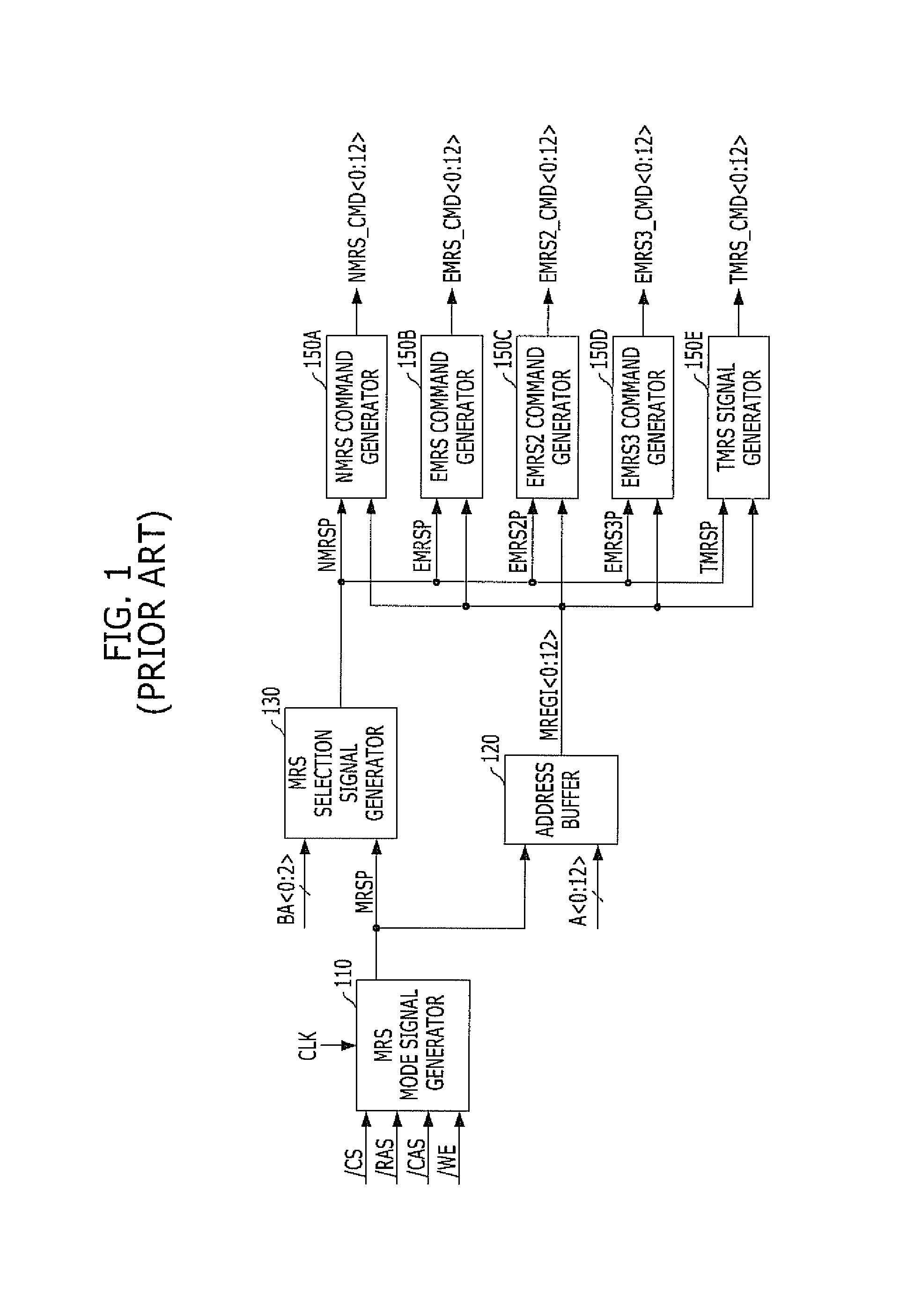
For this reason, the density of the peripheral circuit region becomes high and the size of the peripheral circuit region becomes great, creating a disadvantage in terms of design efficiency.
Since it is expected that more address pins need to be assigned to receive more MRS codes, the size of the semiconductor memory device is expected to increase, which leads to a decrease in cell capacity.
The decoding process not only deteriorates the driving rate of the semiconductor memory device, but also increases the amount of power consumption.

Method used


Image

  • Semiconductor memory device including mode register set and method for operating the same
  • Semiconductor memory device including mode register set and method for operating the same
  • Semiconductor memory device including mode register set and method for operating the same

Examples


Embodiment Construction

[0039]Exemplary embodiments of the present invention will be described below in more detail with reference to the accompanying drawings. The present invention may, however, be embodied in different forms and should not be construed as limited to the embodiments set forth herein. Rather, these embodiments are provided so that this disclosure will be thorough and complete, and will fully convey the scope of the present invention to those skilled in the art. Throughout the disclosure, like reference numerals refer to like parts throughout the various figures and embodiments of the present invention.

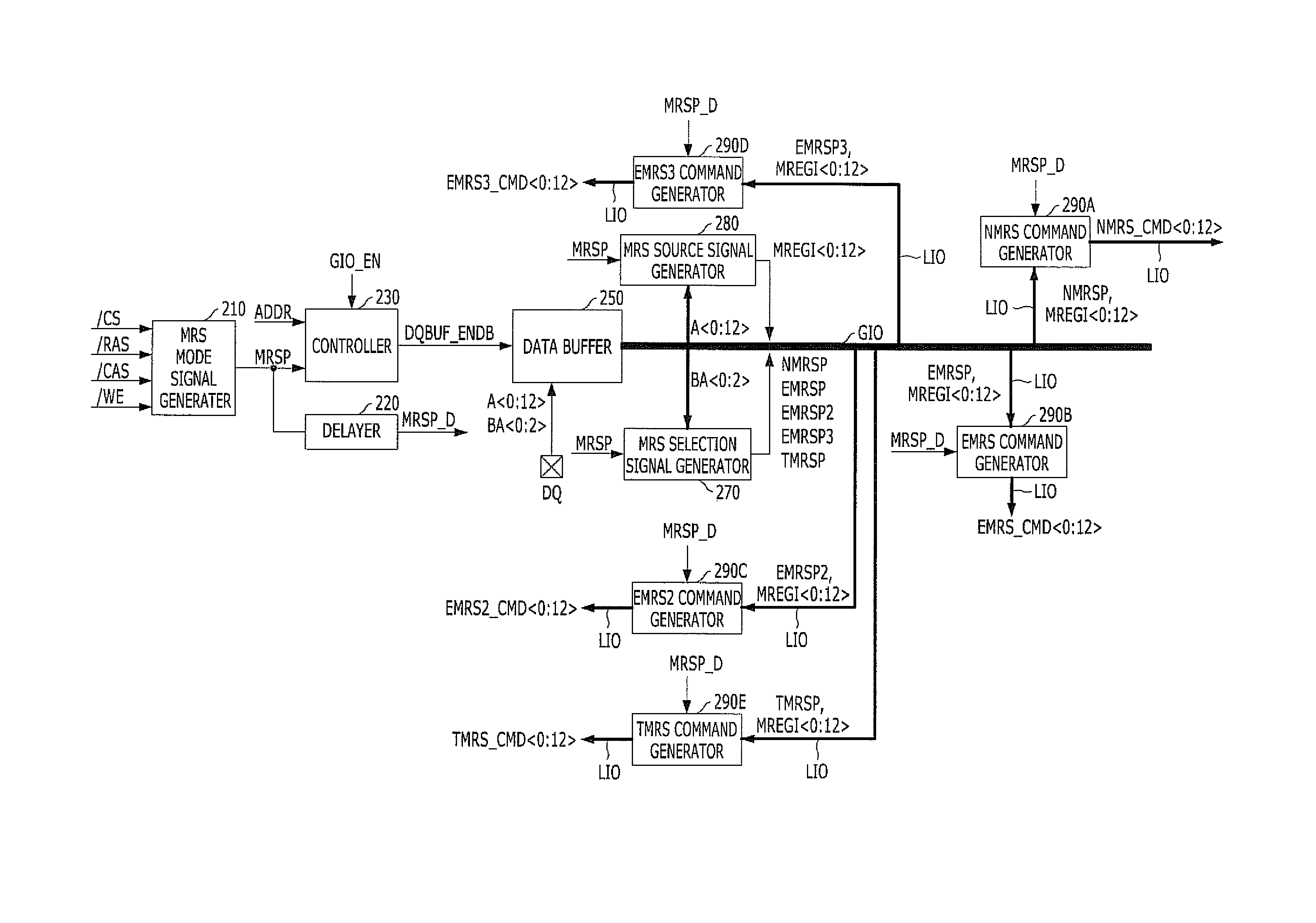
[0040]FIG. 3 is a block diagram of a mode register set (MRS) command generation circuit in accordance with an exemplary embodiment of the present invention, and FIG. 4 is a block diagram of a controller 230 shown in FIG. 3.

[0041]Referring to FIG. 3, the MRS command generation circuit includes an MRS mode signal generator 210, a delayer 220, a controller 230, a data buffer 250, an MRS selecti...


PUM


Abstract

A semiconductor memory device and method for operating the same includes a controller configured to generate a data buffer control signal in a mode register set (MRS) mode, a data buffer configured to buffer and output a plurality of MRS codes inputted through a data pad in response to the data buffer control signal, and a plurality of MRS command generators configured to receive the MRS codes outputted from the data buffer through a data line and generate a plurality of MRS commands based on the received MRS codes.

Description

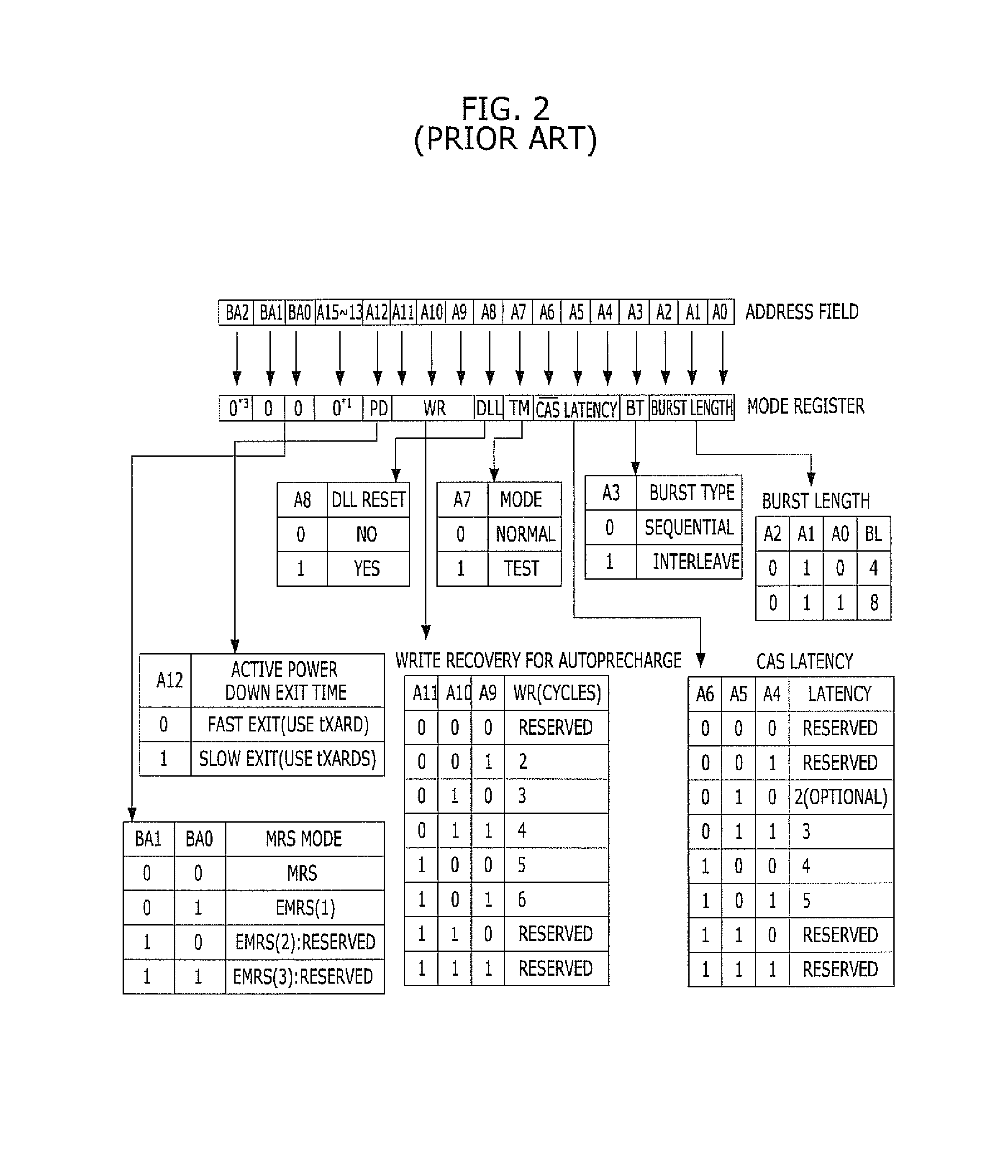
CROSS-REFERENCE TO RELATED APPLICATIONS[0001]The present application claims priority of Korean Patent Application No. 10-2010-0136881, filed on Dec. 28, 2010, which is incorporated herein by reference in its entirety.BACKGROUND[0002]1. Field of the Invention[0003]Exemplary embodiments of the present invention relate to a semiconductor memory device and method for operating the same, and more particularly, to a semiconductor memory device including a mode register set.[0004]2. Description of the Related Art[0005]A register set (RS) is generally used for an operation of setting a particular mode among the operations of a Dynamic Random Access Memory (DRAM) device. Examples of an RS include a mode register set (MRS) and an extended mode register set (EMRS).[0006]The MRS and EMRS set the DRAM device at a particular operation mode based on an MRS code applied through an address pin along with a mode register set command, and the established mode is maintained until a power source is no l...

Claims


Application Information

Patent Timeline
Patent Type & Authority Patents(United States)
IPC IPC(8): G11C8/00G11C7/10
CPCG11C7/1045G11C7/1063G11C11/4093G11C11/4096
Inventor KU, KIE-BONG
Owner SK HYNIX INC
Why Eureka
Eureka Blog
Learn More