Dense finFET SRAM

a technology of static random access memory and finfet logic, which is applied in the direction of transistors, electrical devices, semiconductor devices, etc., can solve the problems of increasing the size of sram cells, and affecting the stability of the finfet logi

Active Publication Date: 2014-09-02
GLOBALFOUNDRIES U S INC
View PDF10 Cites 38 Cited by
  • Summary
  • Abstract
  • Description
  • Claims
  • Application Information

AI Technical Summary

Problems solved by technology

However, the formation of finFET SRAM (static random-access memory) and finFET logic pose new challenges.
One challenge is that some devices (e.g., logic FETs, multiple-finger pull down FETs / pass gate FETs) require epitaxy and a merged source / drain region while other devices (e.g., pull up FETs) only require epitaxy over the source / drain region, without the merging.
Unfortunately, dummy fins result a number of problems, such as an increase in SRAM cell size and tight overlay control in fin patterning (removing dummy fin).
For 10 nm nodes, there is no known solution for forming SRAM finFETs with fin pitch below 20 nm due to the lack of known patterning techniques to meet the tight overlay requirement.

Method used


Image

  • Dense finFET SRAM
  • Dense finFET SRAM
  • Dense finFET SRAM

Examples


Embodiment Construction

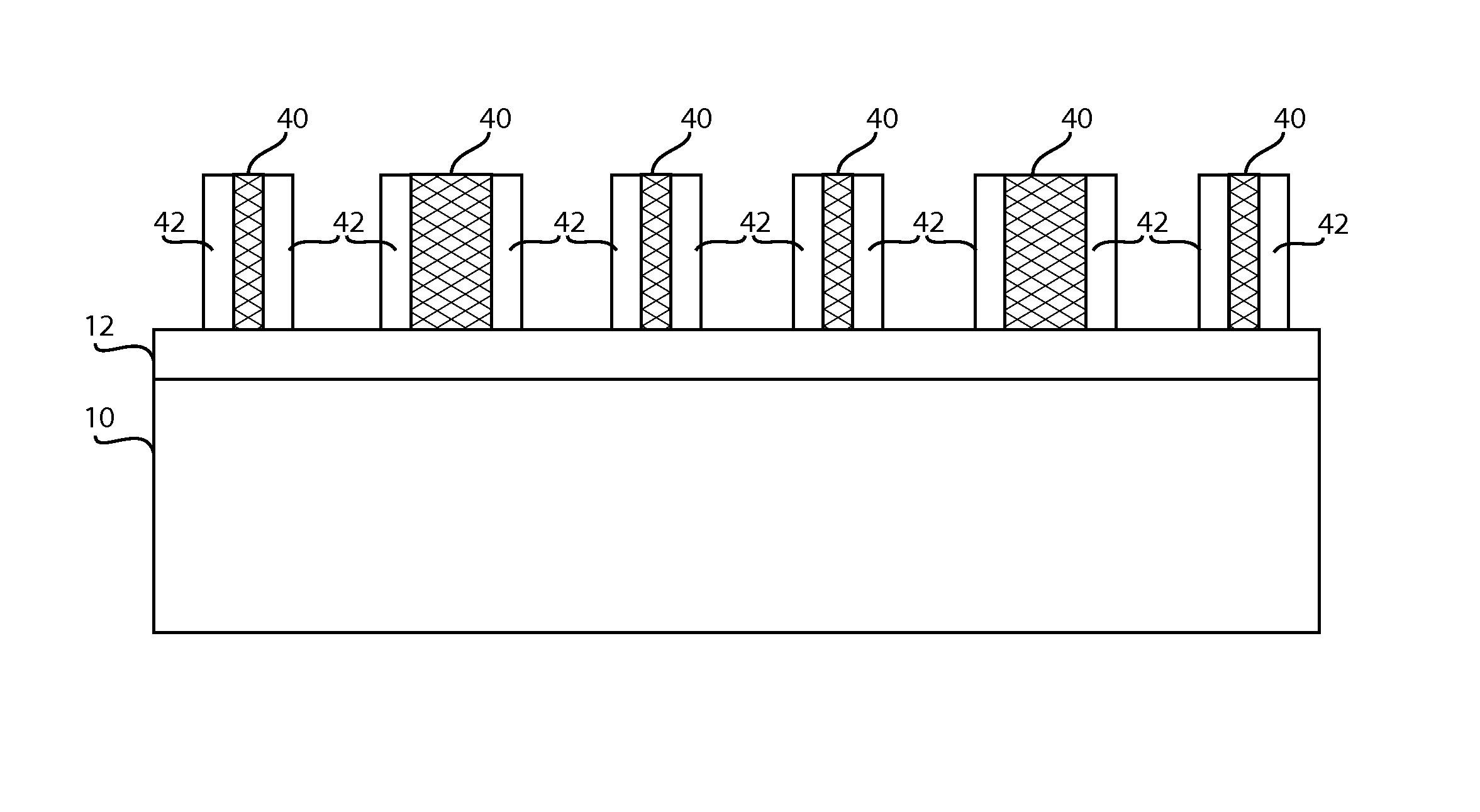
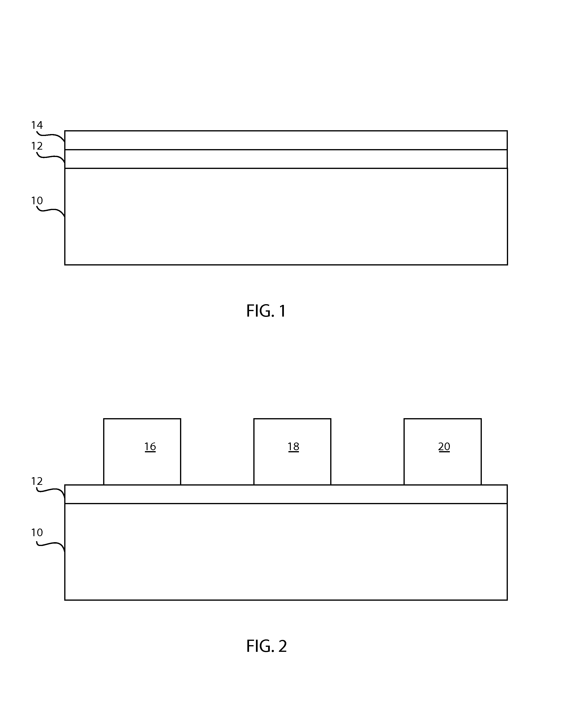
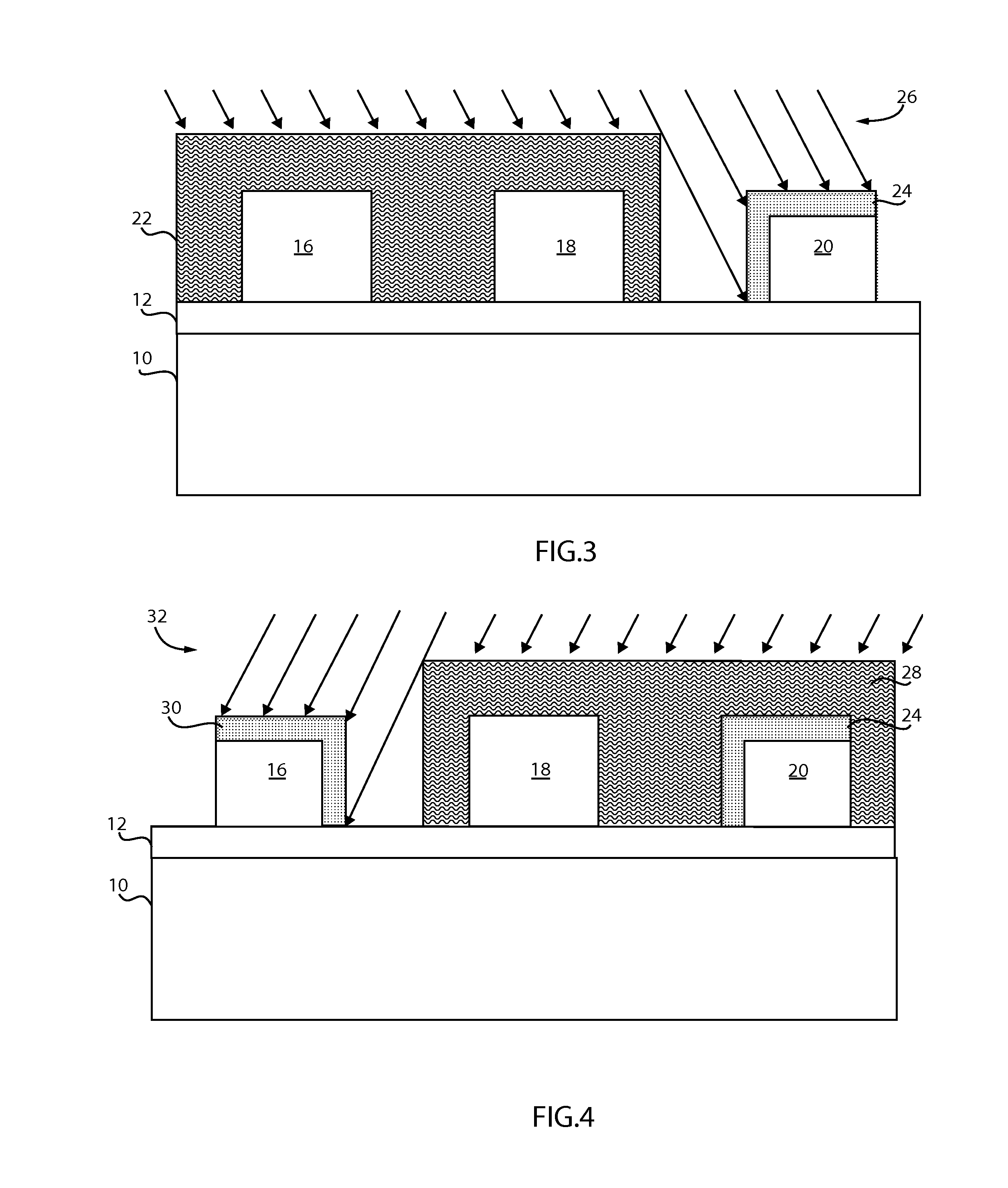
[0027]In accordance with the present principles, a method and device are provided for a dense finFET (fin field effect transistor) SRAM (static random-access memory). Using angled ion implantation into select portions of mandrels, the oxidation rate may be altered. For example, the implanted species may include fluorine to enhance the oxidation rate of exposed portions, or nitrogen to reduce the oxidation rate of exposed portions. Other ion types are also contemplated. Next, oxidation is performed to form thick oxide and thin oxide, according to the implanted ion type. A top layer of the oxidized portions are removed to the underlying mandrel layers, and then the mandrels are removed. Spacers are formed around the remaining oxidized portions and the remaining oxidized portions are removed. The spacers are employed as a mask to form fins. Advantageously, the present principles provide fins with a dense fin pitch which enables both merged fins and unmerged fins without the use of dumm...


PUM


Abstract

A method for fabricating the device includes patterning a first structure and a second structure on a semiconductor device. A first angled ion implantation is applied to the second structure such that the first structure is protected and a second angled ion implantation is applied to the first structure such that the second structure is protected, wherein exposed portions of the first and second structures have an altered rate of oxidation. Oxidation is performed to form thicker or thinner oxide portions on the exposed portions of the first and second structures relative to unexposed portions of the first and second structures. Oxide portions are removed to an underlying layer of the first and second structures. The first and second structures are removed. Spacers are formed about a periphery of remaining oxide portions. The remaining oxide portions are removed. A layer below the spacers is patterned to form integrated circuit features.

Description

BACKGROUND[0001]1. Technical Field[0002]The present invention relates to integrated circuit processing, and more particularly to dense fin field effect transistor static random-access memory.[0003]2. Description of the Related Art[0004]FinFETs (fin field effect transistors) have become a viable device architecture for 22 nm nodes and beyond. However, the formation of finFET SRAM (static random-access memory) and finFET logic pose new challenges. One challenge is that some devices (e.g., logic FETs, multiple-finger pull down FETs / pass gate FETs) require epitaxy and a merged source / drain region while other devices (e.g., pull up FETs) only require epitaxy over the source / drain region, without the merging. Conventionally, dummy fins are utilized to accommodate the merge / unmerge issue. Unfortunately, dummy fins result a number of problems, such as an increase in SRAM cell size and tight overlay control in fin patterning (removing dummy fin).[0005]For 10 nm nodes, there is no known solut...

Claims


Application Information

Patent Timeline
Patent Type & Authority Patents(United States)
IPC IPC(8): H01L29/78H01L29/66
CPCH01L21/823431H01L29/6681H01L21/845H01L27/1211H01L21/32155H01L27/1104H01L27/0886H01L27/0207H01L21/3086H01L29/66803H10B10/12
Inventor CHENG, KANGGUODORIS, BRUCE B.KHAKIFIROOZ, ALISHAHIDI, GHAVAM G.
Owner GLOBALFOUNDRIES U S INC
Why Eureka
Try Eureka