Static memory and memory cell thereof

a static memory and memory cell technology, applied in static storage, information storage, digital storage, etc., can solve the problems of no p-type transistor for performing such an operation, voltage on the storage point st, and inability to reliably control the writing process, so as to achieve the effect of reducing the channel width of the transistor in the static memory cell, reducing the time required for writing data, and improving the writing efficiency of the static memory

Inactive Publication Date: 2014-09-16
NAT CHIAO TUNG UNIV
View PDF11 Cites 28 Cited by
  • Summary
  • Abstract
  • Description
  • Claims
  • Application Information

AI Technical Summary

Benefits of technology

[0014]As described above, in a static memory cell provided by the present invention, the time required for writing data is effectively shortened, so that the writing efficiency of a static memory is improved. Additionally, through the structure of a static memory cell provided by the present invention, the channel widths of the transistors in the static memory cell are effectively reduced, so that the surface area of a static memory is reduced. Moreover, in a static memory cell provided by the present invention, the power consumption is effectively reduced, so that the power consumed by the system chip in an application of an embedded memory can be greatly reduced.

Problems solved by technology

However, when data of logic 1 is to be written, there is no P-type transistor for performing such an operation.
As a result, the writing process may be affected by noises and become unreliable.
In addition, when a data writing operation is performed on the static memory cell 100, the voltage on the storage point ST for storing data is also affected by the voltage division effect of the transistors M5 and M3, and when the transistor M3 offers a high driving capability, the voltage on the storage point ST is low therefore is easily affected by noises.
Thus, the static memory cell 100 cannot work with a low reference operating power supply VDD.

Method used


Image

  • Static memory and memory cell thereof
  • Static memory and memory cell thereof
  • Static memory and memory cell thereof

Examples


Embodiment Construction

[0022]Reference will now be made in detail to the present preferred embodiments of the invention, examples of which are illustrated in the accompanying drawings. Wherever possible, the same reference numbers are used in the drawings and the description to refer to the same or like parts.

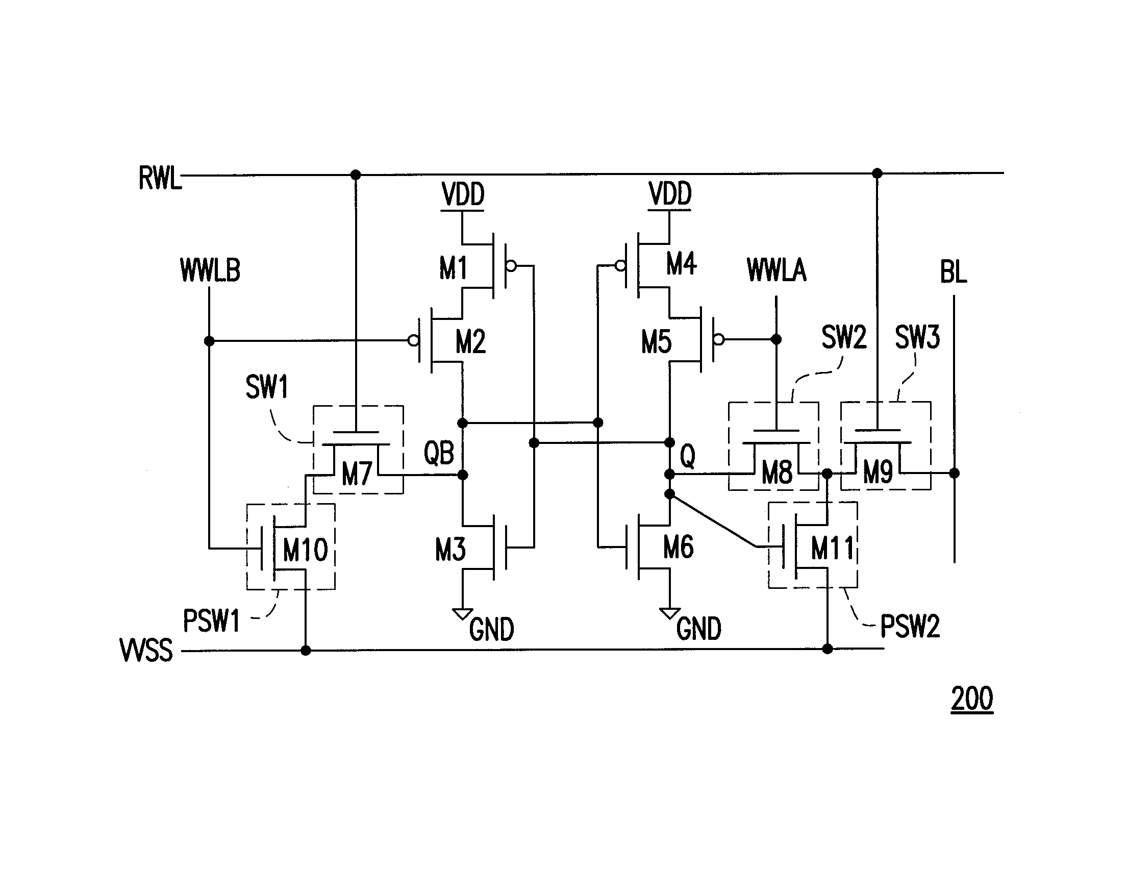
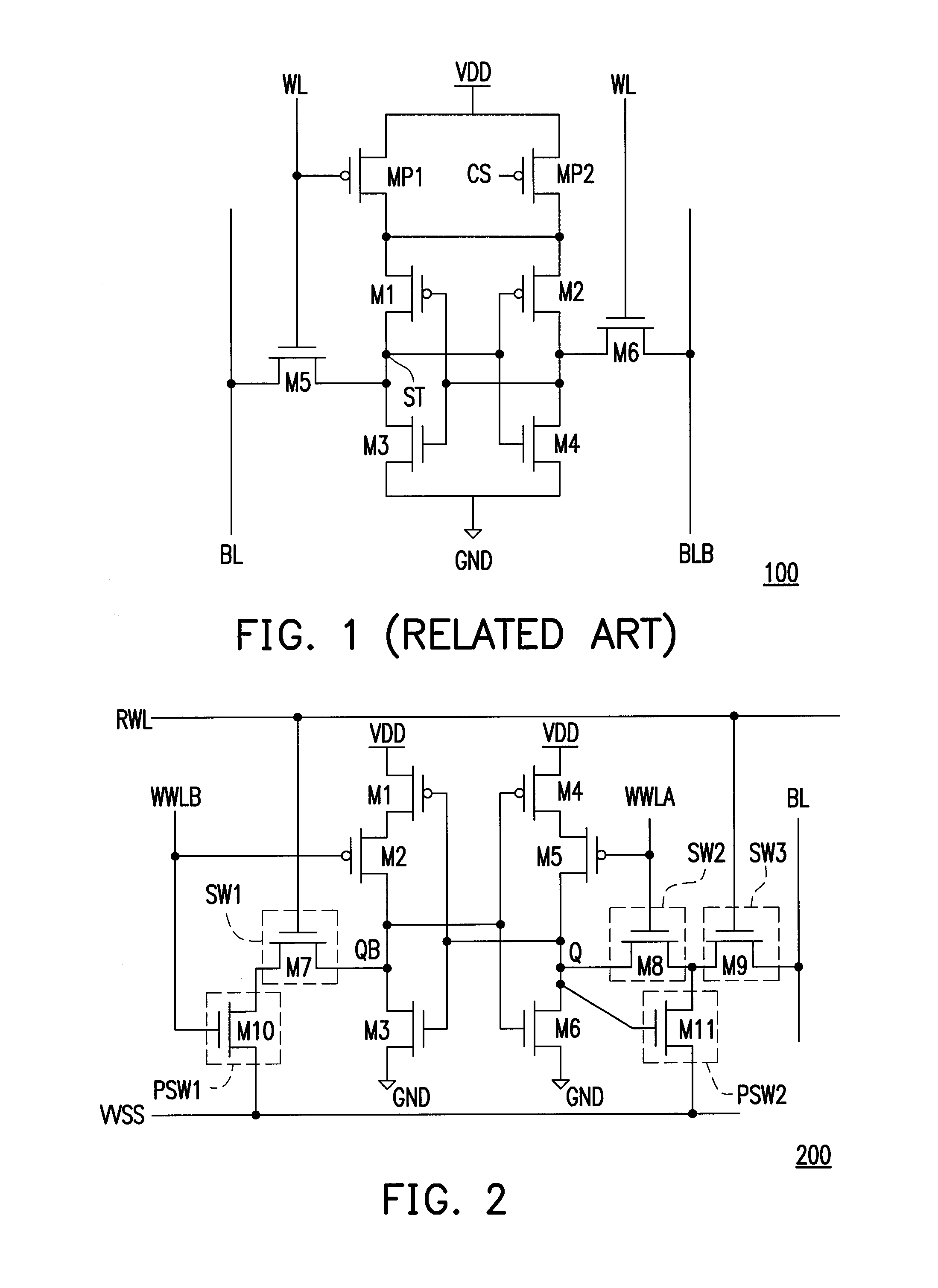
[0023]FIG. 2 is a diagram of a static memory cell 200 according to an embodiment of the present invention. Please refer to FIG. 2, the static memory cell 200 includes transistors M1-M6, switches SW1-SW3, and pull-down switches PSW1-PSW2. The first terminal of the transistor M1 is coupled to a reference operating power supply VDD. The first terminal of the transistor M2 is coupled to the second terminal of the transistor M1, the second terminal of the transistor M2 is coupled to an output terminal QB, and the control terminal of the transistor M2 receives a write word line signal WWLB. The first terminal of the transistor M3 is coupled to the output terminal QB, the control terminal of the transistor ...


PUM


Abstract

A static memory and a static memory cell are provided. The static memory cell includes a first transistor, a second transistor, a third transistor, a fourth transistor, a fifth transistor, a sixth transistor, a first switch, a second switch, a third switch, a first pull-down switch, and a second pull-down switch. When a data writing operation is performed, the latching capability of the latch circuit constituted by the first to the sixth transistors is disabled by turning off the second transistor or the fifth transistor, so that the speed of the data writing operation is increased and the data writing performance is improved. The first switch and the second switch provide a path for reading or writing data, and the third switch is coupled to a bit line for receiving data from or transmitting data to the bit line.

Description

CROSS-REFERENCE TO RELATED APPLICATION[0001]This application claims the priority benefit of Taiwan application serial no. 102114386, filed on Apr. 23, 2013. The entirety of the above-mentioned patent application is hereby incorporated by reference herein and made a part of this specification.BACKGROUND OF THE INVENTION[0002]1. Field of the Invention[0003]The present invention generally relates to a static memory cell and a static memory, and more particularly, to a static memory cell which can work with a sub-threshold voltage and a static memory.[0004]2. Description of Related Art[0005]FIG. 1 is a circuit diagram of a conventional static memory cell 100. Please refer to FIG. 1, the static memory cell 100 includes transistors M1-M6 and transistors MP1 and MP2. When a data writing operation is performed on the static memory cell 100, the transistors MP1 and MP2 are turned off through a transverse word line signal WL and a column selection signal CS, and the transistors M1-M4 are cut ...

Claims


Application Information

Patent Timeline
Patent Type & Authority Patents(United States)
IPC IPC(8): G11C11/00G11C11/412
CPCG11C11/412
Inventor JOU, SHYH-JYETU, MING-HSIENHU, YU-HAOCHUANG, CHING-TECHIU, YI-WEI
Owner NAT CHIAO TUNG UNIV
Why Eureka
Try Eureka