Array substrate for in-plane switching mode liquid crystal display device
a liquid crystal display and array substrate technology, applied in the field of array substrates for in-plane switching mode liquid crystal display devices, can solve the problems of complex fabrication process, deterioration of subsequent process such as rubbing process, and inability to meet the requirements of the device, so as to achieve the effect of improving the quality of the display
- Summary
- Abstract
- Description
- Claims
- Application Information
AI Technical Summary
Benefits of technology
Problems solved by technology
Method used
Image


Examples
Embodiment Construction
[0035]Reference will now be made in detail to embodiments of the present invention, examples of which are illustrated in the accompanying drawings. Wherever possible, similar reference numbers will be used to refer to the same or similar parts.
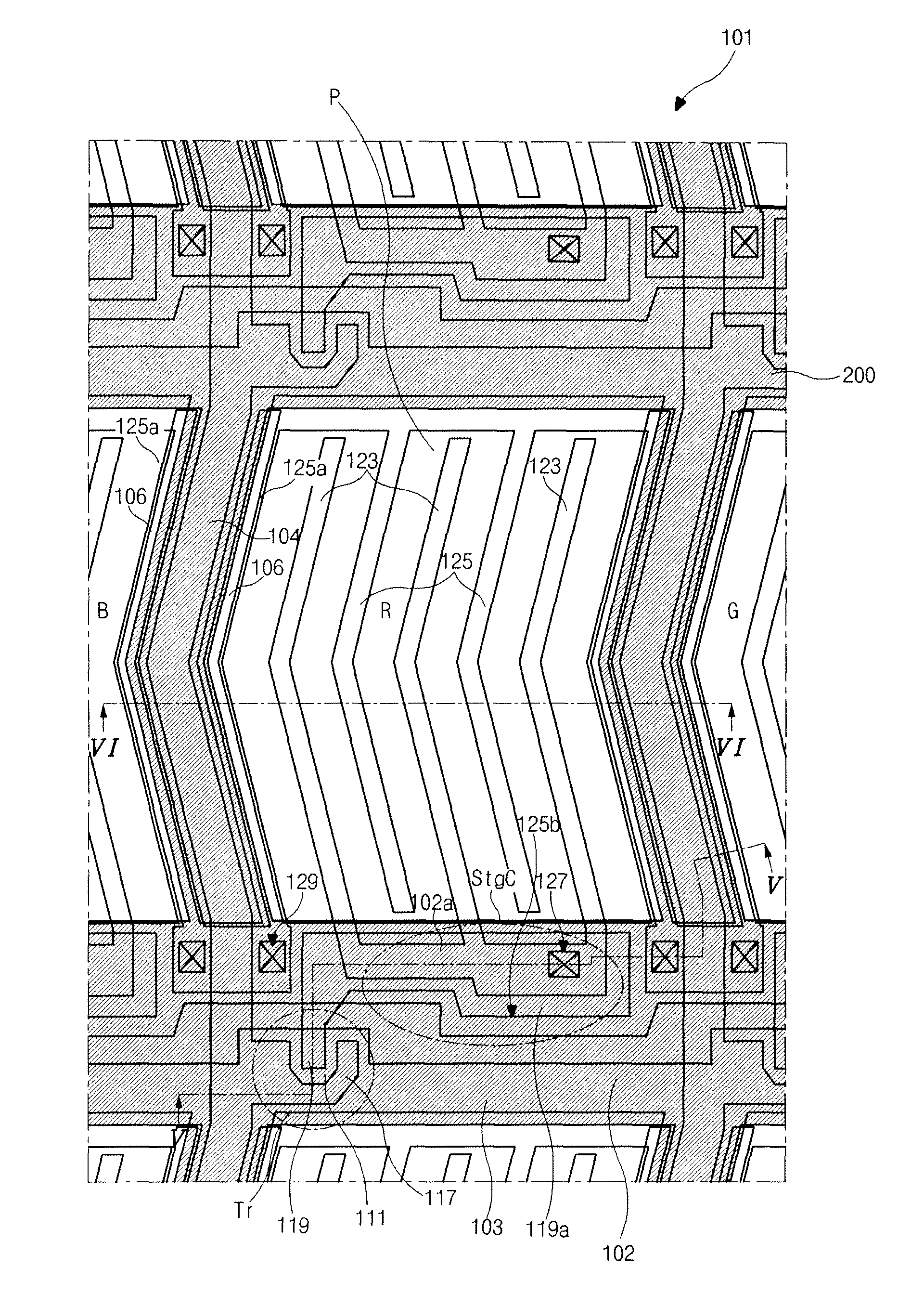
[0036]FIG. 4 is a plane view showing an array substrate for a color filter on thin film transistor type in-plane switching mode liquid crystal display device according to an embodiment of the present invention, FIG. 5 is a cross-sectional view taken along a line V-V of FIG. 4, and FIG. 6 is a cross-sectional view taken along a line VI-VI of FIG. 4.
[0037]In FIG. 4, a common line 102, a gate line 103 and a data line 104 are formed on a substrate 101. The common line 102 is parallel to the gate line 103, and the gate line 103 and the data line 104 cross each other to define a pixel region P. A thin film transistor (TFT) Tr is connected to the gate line 103 and the data line 104. The TFT Tr includes a gate electrode 111, a gate insulating layer 11...
PUM
| Property | Measurement | Unit |
|---|---|---|
| resistivity | aaaaa | aaaaa |
| optical density | aaaaa | aaaaa |
| optical density | aaaaa | aaaaa |
Abstract
Description
Claims
Application Information