Method of manufacturing a hollow surface mount type electronic component

a technology of electronic components and surface mounts, which is applied in the direction of adhesive processes with surface pretreatment, electrical apparatus casings/cabinets/drawers, hermetically sealed casings, etc., can solve the problems of high cost of sealing conventional smd electronic components, and increasing the rejection ratio of manufacturing smd electronic components. , to achieve the effect of convenient manufacturing, high volume ratio and preferred quality

Inactive Publication Date: 2014-09-30
YANG CHIN CHI
View PDF11 Cites 0 Cited by
  • Summary
  • Abstract
  • Description
  • Claims
  • Application Information

AI Technical Summary

Benefits of technology

[0008]The main objective of the present invention is to provide a method of manufacturing a hollow surface mount type (SMD) electronic component, and more particularly to a method that can be manufactured conveniently and can provide a preferred quality and a high volume ratio.

Problems solved by technology

The hermetic sealing method uses metals or ceramics to seal the conventional SMD electronic components, and this can provide a high stability, but the cost of sealing the conventional SMD electronic components is high.
Although the non-hermetic sealing method can provide a protective effect to the conventional SMD electronic components, the high temperature of the heated resin in the sealing process may destroy conventional SMD electronic components.
The solidified resin also causes residual stress on the conventional SMD electronic components so increasing the reject ratio of manufacturing the SMD electronic components.
In addition, the resin is soft and easily deformed, when the resin is impacted, the SMD electronic components inside the resin may be broken.

Method used


Image

  • Method of manufacturing a hollow surface mount type electronic component
  • Method of manufacturing a hollow surface mount type electronic component
  • Method of manufacturing a hollow surface mount type electronic component

Examples


Embodiment Construction

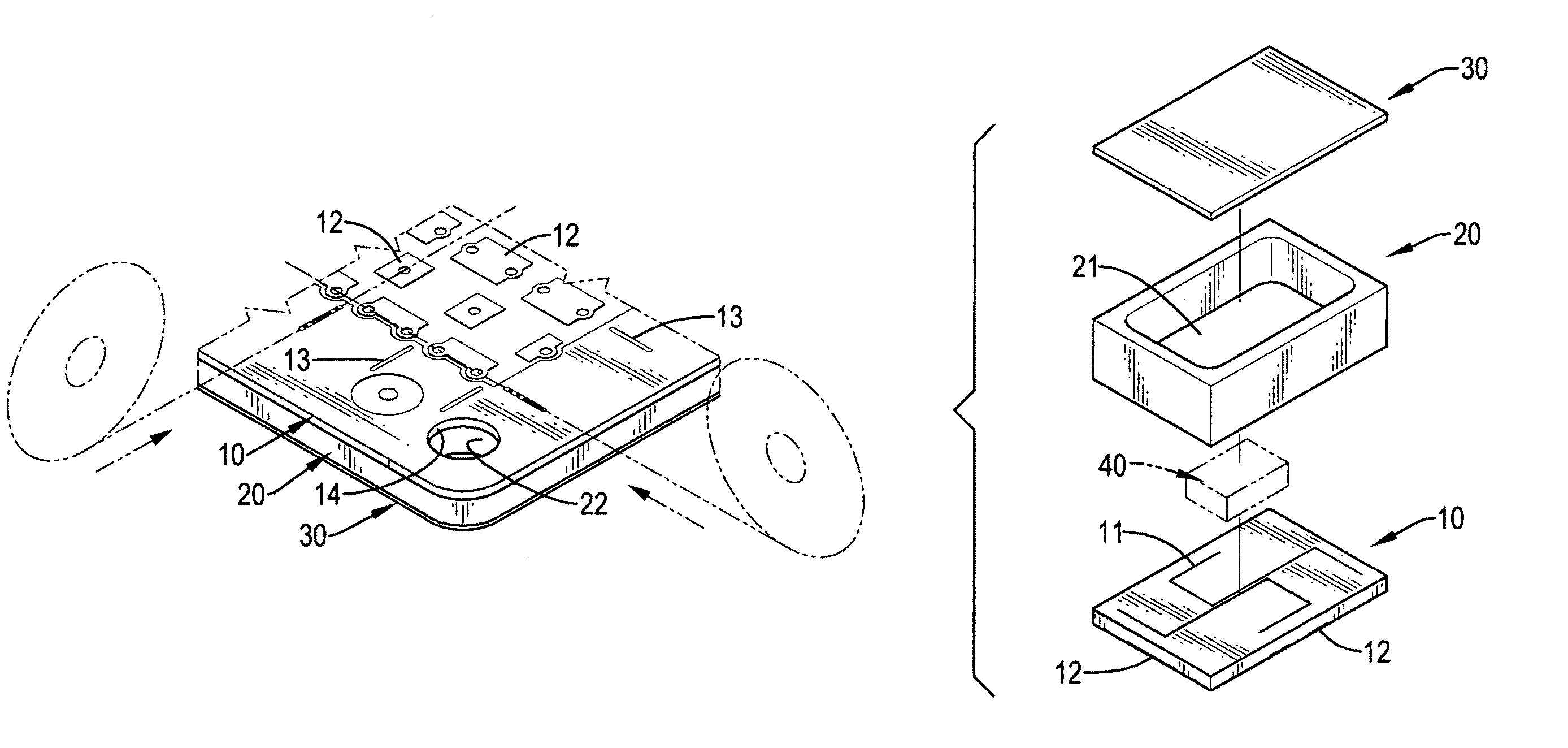
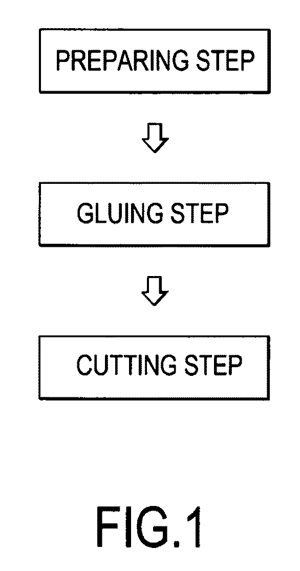
[0019]With reference to FIGS. 1 and 2, a method of manufacturing a hollow surface mount type (SDM) electronic component in accordance with the present invention comprises a preparing step, a gluing step and a cutting step.

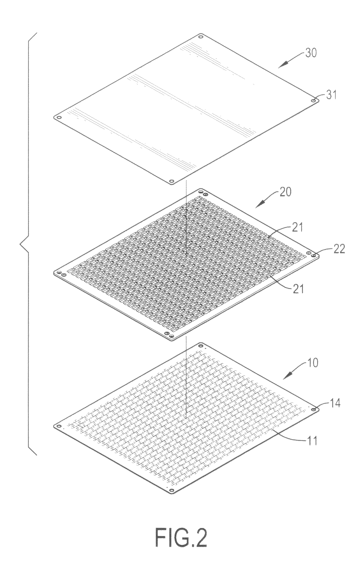
[0020]With further reference to FIG. 3, the preparing step comprises preparing a baseboard (10), a clapboard (20) and a cover board (30), cleaning and drying the boards (10, 20, 30), mounting multiple circuit segments (11) on a top face of the baseboard (10) at intervals, mounting multiple conducting points (12) on a bottom face of the baseboard (10) at intervals and connecting to the circuit segments (11) and marking multiple cutting lines (13) on the bottom face of the baseboard (10) around the conducting points (12).

[0021]After the cutting lines (13) are marked on the bottom face of the baseboard (10), multiple through holes (21) are formed on the clapboard (20) corresponding to the circuit segments (11) on the baseboard (10) to form a rib between each pair of a...


PUM

PropertyMeasurementUnit
temperatureaaaaaaaaaa
conductingaaaaaaaaaa
impedanceaaaaaaaaaa

Abstract

A method of manufacturing a hollow surface mount type electronic component has a preparing step, a gluing step and a cutting step. The preparing step includes preparing a baseboard, a clapboard and a cover board, mounting multiple circuit segments and conducting points on two opposite faces of the baseboard at intervals and boring multiple through holes on the clapboard corresponding to the circuit segments. The gluing step includes mounting multiple electronic elements on the baseboard to connected with the circuit segments, gelatinizing glue on the boards to mount the clapboard between the baseboard and the cover board and pressing the boards by a pressing machine. The cutting step includes cutting the boards by a cutting machine to produce multiple single SDM electronic components.

Description

BACKGROUND OF THE INVENTION[0001]1. Field of the Invention[0002]The present invention relates to a method of manufacturing a hollow surface mount type (SMD) electronic component, and more particularly to a method that can be processed conveniently and can provide a preferred quality and a high capacity ratio.[0003]2. Description of the Prior Arts[0004]In order to meet the tendency of micro-minimizing and simplifying of integrated circuits (IC) and electronic products, plugging type electronic components on a printed circuit board (PCB) have become surface mount type (SMD) electronic components that are mounted on a surface of the printed circuit board. The SMD electronic components have advantages of low impedance, high capacity, miniaturization and long life span. Therefore, the conventional SMD electronic components are applied to motherboards, CD-ROM drives, modems, monitors and so on.[0005]The conventional SMD electronic components are always packaged in a container or in a seal...

Claims


Application Information

Patent Timeline
Patent Type & Authority Patents(United States)
IPC IPC(8): H05K3/30H05K13/04H05K3/36H01L21/50
CPCH01L21/50Y10T29/4913Y10T156/1064Y10T156/1052Y10T29/49128Y10T29/49126Y10T29/49146Y10T156/1082H01L2224/97
Inventor YANG, CHIN-CHI
Owner YANG CHIN CHI
Why Eureka
Try Eureka