Low dielectric photoimageable compositions and electronic devices made therefrom

a composition and low dielectric technology, applied in the field of low dielectric photoimageable compositions and electronic devices made therefrom, can solve the problems of limiting both the thickness and the use of siloxane, the difficulty of processing of liquid or tacky siloxane layers, and the inability to achieve thin coatings, etc., to achieve thicker coatings, improve flexibility and crack resistance, and increase the viscosity of compositions

Active Publication Date: 2014-10-28
MERCK PATENT GMBH
View PDF21 Cites 5 Cited by
  • Summary
  • Abstract
  • Description
  • Claims
  • Application Information

AI Technical Summary

Benefits of technology

[0006]It has been surprisingly found that siloxane based photoresist compositions containing various water soluble polymers provide for improved flexibility and crack resistance as well as increasing the viscosity of the composition to allow for thicker coatings than those obtainable from siloxane based photoresist compositions alone. The composition of the present invention may be a negative tone composition or a positive tone composition.
[0010]In a third embodiment of the current application for patent is disclosed and claimed the compositions of the above embodiments wherein the water soluble organic polymer has a glass transition temperature greater than about 100° C. and a dielectric constant less than about 10 and is present in the composition in an effective amount to improve flexibility in a dried state before and after photoimaging.
[0016]In a further embodiment of the current application for patent is disclosed and claimed a method for forming a dielectric image on a substrate containing the steps of coating the substrate with the composition of the above embodiments, heating the composition to substantially remove solvent, exposing the dried composition to actinic radiation through a photomask, optionally heating the exposed composition to further cure it, developing the composition using an aqueous alkaline developer to remove the unexposed portions of the composition, and optionally heating the resultant exposed and developed composition to further cure it, wherein the water soluble organic polymer is present in an effective amount to provide the desired thickness, flexibility and tack free surface.

Problems solved by technology

Many siloxane polymers in these applications are characterized by a very low glass transition temperature (Tg) which results in liquid or tacky siloxane layers which are very difficult to process.
Attempts to provide siloxane polymers with a high Tg and thus tack free coatings has resulted in brittle layers which are easily cracked, limiting both their use and the thicknesses which can be achieved.
Addition of dimethylsiloxane to silicon polymers, however, results in tacky coatings.
The functionalized polymers suitable in these compositions are generally water insoluble which can lead to problems during development including scumming or overdevelopment of the image when trying to remove the scum.
Typically, adding more siloxane to the composition to increase solids is hampered by stability issues, as well as a limit on the viscosity attainable.

Method used


Image

  • Low dielectric photoimageable compositions and electronic devices made therefrom
  • Low dielectric photoimageable compositions and electronic devices made therefrom
  • Low dielectric photoimageable compositions and electronic devices made therefrom

Examples


example 1

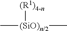
[0048]409.74 g of a 90:10 methyl:phenyl silsesquioxane polymer (69.0% solids in propylene glycol monomethyl ether acetate ((PGMEA)), 29.76 g of poly(vinylpyrrolidone-co-vinylacetate) polymer (50% solids in propylene glycol monomethyl ether (PGME) (available from Sigma-Aldrich), and 29.76 g of Irgacure-108 (20.0% solids in methyl iso-butyl ketone (MIBK); available from Ciba) were dissolved in PGME to achieve 60% of total solids.

[0049]The resulting photoimageable dielectric composition was filtered and spin coated onto a 6 inch silicon wafer and soft baked at 90° C. for 60 seconds to obtain a tack-free, crack-free film with a film thickness of 10.1 microns. The photoresist film was patternwise exposed to broadband light on an Ultratech stepper, and post-exposure baked at 80° C. for 60 seconds. This was followed by 30 second puddle development with a 2.38 wt % tetramethylammonium hydroxide (TMAH) developer to resolve features with a film thickness of 9.6 micron. Cross-sectional Scannin...

example 2

[0053]84.12 g of a 90:10 methyl:phenyl silsesquioxane polymer (69.0% solids in PGMEA), 12.90 g of poly(vinylpyrrolidone-co-vinylacetate)polymer (50% solids in PGME) (available from Sigma-Aldrich), and 1.61 g of Irgacure-108 (20.0% solids in MIBK) were dissolved in PGME to achieve 64.6% of total solids.

[0054]The resulting photoimageable dielectric composition was filtered and spin coated onto a 8 inch silicon wafer and soft baked at 140° C. for 30 seconds to obtain a photoresist film. Then the same formulation was coated on top of the aforementioned wafer again (double coating) and soft baked at 140° C. for 300 seconds to obtain a photoresist film with a film thickness of over 150 microns. The photoresist film was patternwise exposed to broadband light on a Suss Aligner, and post-exposure baked at 80° C. for 80 seconds. This was followed by four times of 90 second puddle development step with a 2.38 wt % TMAH developer to resolve features with a film thickness of 130 micron. X-SEM re...

example 3

[0056]164.39 g of a 90:10 methyl:phenyl silsesquioxane polymer (69.0% solids in PGMEA), 11.94 g of polyvinylpyrrolidone polymer (50% solids in PGME) (available from Sigma-Aldrich), and 11.94 g of Irgacure-108 (20.0% solids in MIBK) were dissolved in PGME to achieve 60% of total solids. The resulting photoimageable dielectric composition was filtered and spin coated onto a 6 inch silicon wafer and soft baked at 95° C. for 60 seconds to obtain a photoresist film with a film thickness of 10.5 microns. The photoresist films were patternwise exposed to broadband light on an Ultratech stepper, and post-exposure baked at 90° C. / 60 s, 95° C. / 60 s, and 100° C. / 60 s, respectively. This was followed by a 30 second puddle development step with a 2.38 wt % TMAH developer to resolve features with a film thickness of approximately 10 microns. The resulting patterned dielectric film was then baked at 250° C. for 60 minutes on a hotplate under a nitrogen atmosphere.

[0057]The cured dielectric films o...


PUM

PropertyMeasurementUnit
glass transition temperatureaaaaaaaaaa
dielectric constantaaaaaaaaaa
Tgaaaaaaaaaa

Abstract

This invention relates generally to silicon based photoresist compositions that can be used in forming low k dielectric constant materials suitable for use in electronic devices, methods of their use and the electronic devices made therefrom.

Description

BACKGROUND OF THE INVENTION[0001]This invention relates generally to silicon based photoresist compositions that can be used in forming low k dielectric constant materials suitable for use in electronic devices, methods of their use and the electronic devices made therefrom.[0002]As electronic devices become smaller, there is a continuing desire in the electronics industry to increase the circuit density in electronic components, e.g., integrated circuits, circuit boards, multichip modules, chip test devices, and the like without degrading electrical performance, e.g., crosstalk or capacitive coupling, and also to increase the speed of signal propagation in these components. One method of accomplishing these goals is to reduce the dielectric constant of the interlayer insulating material used in the components.[0003]Siloxane based materials have been identified and used as low k materials for reducing the dielectric constant of such interlayer insulating material. Generally a siloxa...

Claims


Application Information

Patent Timeline
Patent Type & Authority Patents(United States)
IPC IPC(8): G03F7/11G03F7/00
CPCG03F7/0757H01L23/5329G03F7/038H01L21/02282G03F7/0758C08L83/04H01L21/02126H01L2924/0002Y10T428/24802H01L2924/00
Inventor ZHANG, RUZHIKIM, JIHOONPATEL, BHARATKUMAR K.WOLFER, ELIZABETH
Owner MERCK PATENT GMBH
Why Eureka
Try Eureka