Perovskite oxide film and ferroelectric film using the same, ferroelectric device, and method for manufacturing perovskite oxide film

a technology of perovskite oxide and ferroelectric film, which is applied in the direction of device material selection, niobium compound, record information storage, etc., can solve the problems of difficult to obtain a single crystal of good crystallinity and extremely difficult composition control of potassium niobate mixed crystals, etc., to achieve good crystallinity, reduce the effect of composition shift and composition shi

Active Publication Date: 2014-10-28
FUJIFILM CORP +1
View PDF11 Cites 0 Cited by
  • Summary
  • Abstract
  • Description
  • Claims
  • Application Information

AI Technical Summary

Benefits of technology

[0011]The present invention has been developed in view of the circumstances described above, and it is an object of the present invention to provide a potassium niobate mixed crystal perovskite oxide thick film with little composition shift and good crystallinity.
[0025]In low-temperature film forming for potassium niobate mixed crystal perovskite oxide films by hydrothermal synthesis, the present inventors have earnestly studied factors that may affect the composition and found out film forming conditions for forming a potassium niobate mixed crystal perovskite oxide film with little composition shift under a relative low temperature less than Curie temperature. Therefore, the present invention may provide, on a substrate, a potassium niobate mixed crystal perovskite oxide film having a film thickness of not less than 5 μm with little composition shift, good crystallinity, and less defects, such as cracks and the like.

Problems solved by technology

1646-1649, 2009, the composition control for the mixed crystal of potassium niobate is extremely difficult, whereby it is difficult to obtain a single crystal of good crystallinity.

Method used


Image

  • Perovskite oxide film and ferroelectric film using the same, ferroelectric device, and method for manufacturing perovskite oxide film
  • Perovskite oxide film and ferroelectric film using the same, ferroelectric device, and method for manufacturing perovskite oxide film
  • Perovskite oxide film and ferroelectric film using the same, ferroelectric device, and method for manufacturing perovskite oxide film

Examples


example 1

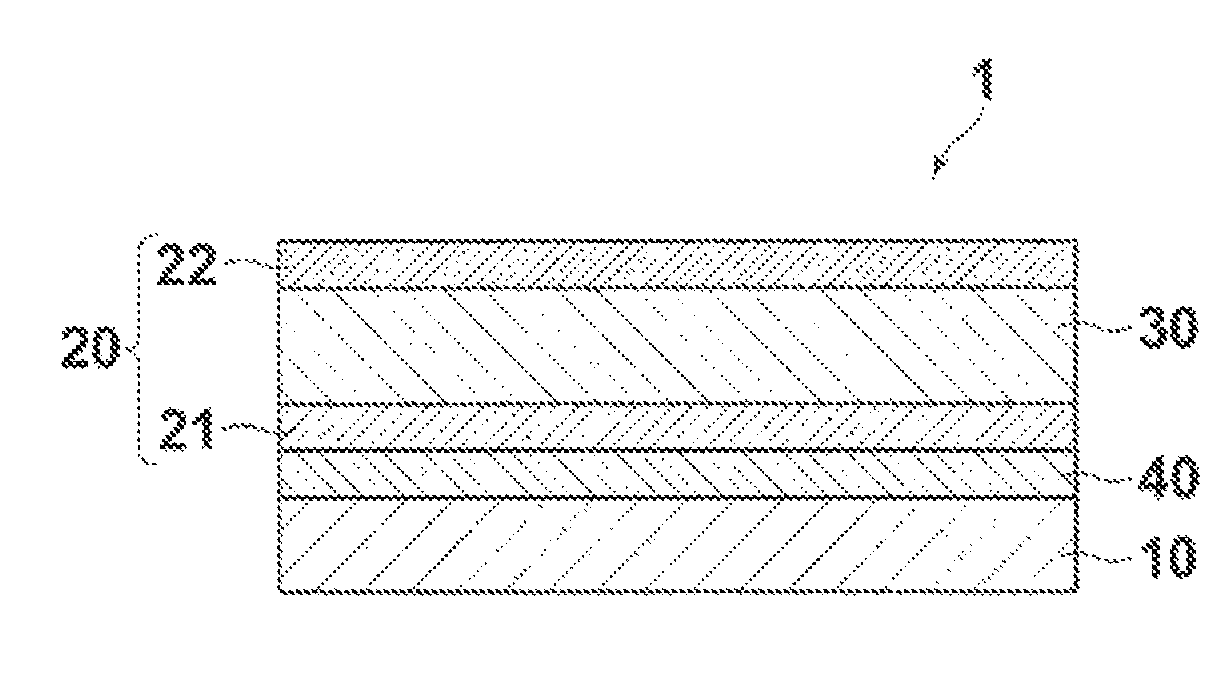
[0092]A (100) SrTiO3 (STO) substrate with a thickness of 500 μm was prepared and a SrRuO3 (SRO) back contact electrode was formed on the surface of the substrate with a thickness of about 60 nm by sputtering. In forming the electrode, a commercially available SRO target was used as the target under the following film forming conditions: output power of 60 W; substrate temperature of about 600° C.; deposition pressure of 27 Pa; argon-oxygen ratio of 20 / 5; substrate-target distance of 120 mm; and deposition time of about 220 minutes.

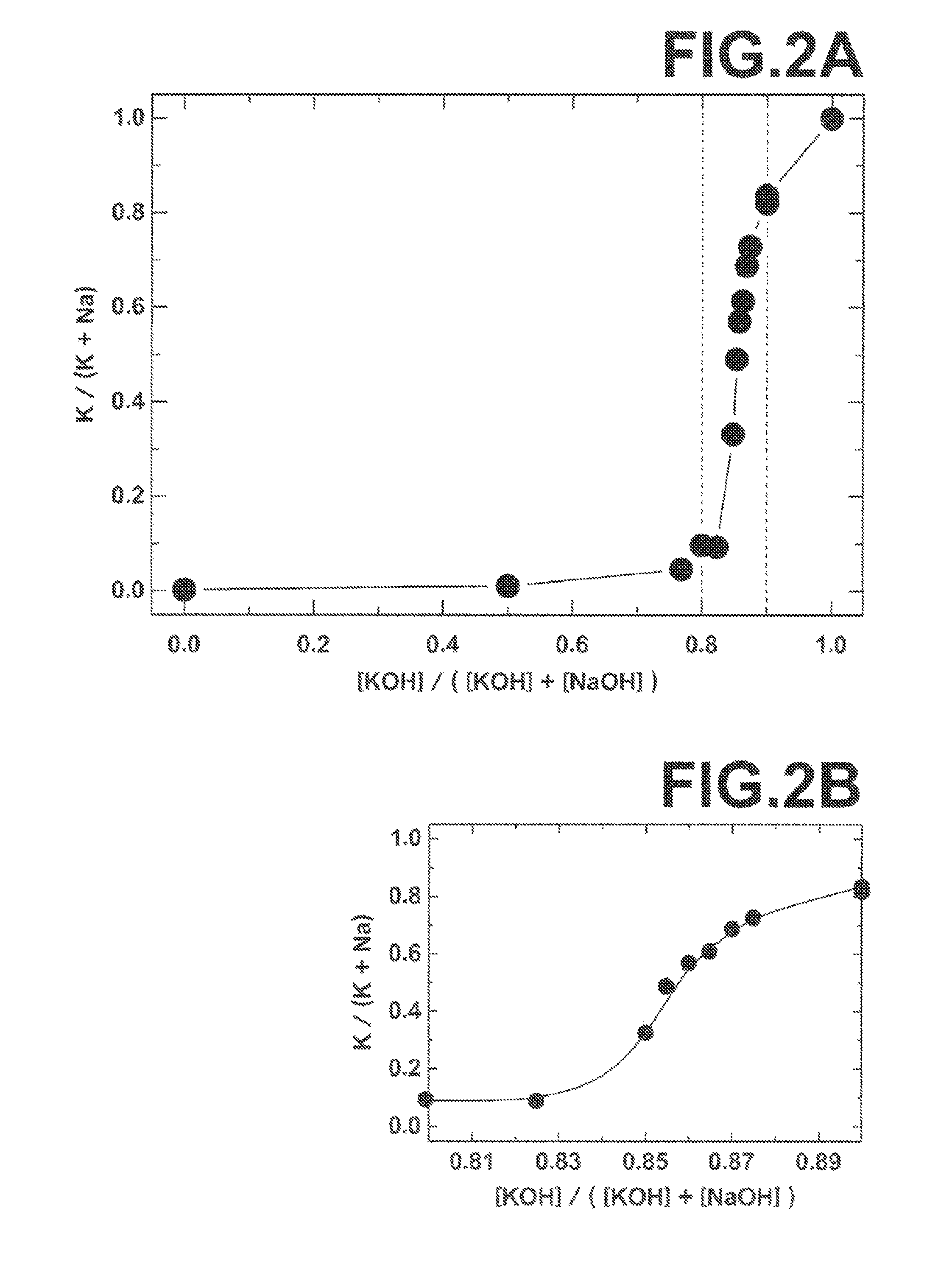
[0093]Then, reaction solutions were prepared. 9×10⁻⁴ mol of Nb2O5 powder, 7 mol / l of KOH, and 7 mol / l of NaOH were provided and mixed to prepare for a 20 ml of reaction solution having each of the predetermined compositions shown in Table 1.

[0094]Each reaction solution shown in Table 1 was put into a temperature controllable reaction vessel and the temperature was controlled such that the temperature of each reaction solution becomes 240° C. Then the subst...

example 2

[0101]As the substrate, following three substrates were provided.[0102] inconel substrate (300 μm thickness)[0103] SrRuO3 (SRO) / inconel substrate (300 μm thickness)

[0104]Film forming conditions: A SrRuO3 (SRO) was formed on a 300 μm thick inconel substrate by sputtering with a thickness of about 120 nm as a buffer layer. A commercially available SRO target was used as the target, Film forming conditions: output power of 40 W; substrate temperature of about 600° C.; deposition pressure of 8 Pa; argon-oxygen ratio of 70 / 30; substrate-target distance of 70 mm; and deposition time of about 60 minutes.[0105] SRO / La2NiO4 (LNO) / inconel substrate (300 μm thickness)

[0106]Film forming conditions: A SRO (film thickness of about 120 nm) / La2NiO4 (LNO) (film thickness of about 150) was formed on a 300 μm thick inconel substrate by sputtering as a buffer layer. A commercially available SRO and LNO targets were used as the targets. With respect to the LNO, film forming was performed under three-sta...

example 3

[0116]A 300 μm thick inconel substrate formed in a cantilever shape by wire electrical discharge machining was provided and SrRuO3(SRO) was formed on the surface thereof with a thickness of about 120 nm as a buffer layer. The film forming conditions were similar to those of the substrate 2 in Example 2.

[0117]Then, a 20 ml of reaction solution having the same composition as that of No. 12 in Table 1 was prepared, and a (K, Na)NbO3 film was formed on the SRO buffer layer with a thickness of about 6 μm as in each substrate in Example 2. The results of composition analysis performed in the same manner as in Example 1 showed that the composition of K / (K+Na) in the film was 0.88.

[0118]Next, an Au upper electrode was provided on the (K, Na)NbO3 film by low vacuum vapor deposition, thereby providing a measuring sample (cantilever) for piezoelectric property evaluation. Note that the sample was not subjected to polarization treatment. The piezoelectric property evaluation was performed by a ...


PUM

PropertyMeasurementUnit
thicknessaaaaaaaaaa
lattice constantaaaaaaaaaa
thicknessaaaaaaaaaa

Abstract

A perovskite oxide film is formed on a substrate, in which the perovskite oxide film has an average film thickness of not less than 5 μm and includes a perovskite oxide represented by a general formula (P) given below:(K1-w-x,Aw,Bx)(Nb1-y-z,Cy,Dz)O3  (P),where: 0<w<1.0, 0≦x≦0.2, 0≦y<1.0, 0≦z≦0.2, 0<w+x<1.0, A is an A-site element having an ionic valence of 1 other than K, B is an A-site element, C is a B-site element having an ionic valence of 5, D is a B-site element, each of A to D is one kind or a plurality of kinds of metal elements.

Description

CROSS REFERENCE TO RELATED APPLICATIONS[0001]This non-provisional application is a Continuation of International Application No. PCT / JP2011 / 005881 filed on Oct. 20, 2011, which claims the benefit of Japanese Patent Application Nos. 2010-238592 filed on Oct. 25, 2010 and 2011-065517 filed on Mar. 24, 2011, both are filed in Japan. The entire contents of all of the above applications are hereby incorporated by reference.TECHNICAL FIELD[0002]The present invention relates to an I-V perovskite oxide film and ferroelectric film using the same, a ferroelectric device, and a method for manufacturing the I-V perovskite oxide film.BACKGROUND ART[0003]Today, with an increasing interest in the environmental impact, switching to a non-lead based system has been actively conducted for piezoelectric films used for piezoelectric actuators, ultrasound probes, pressure sensors, and the like. As one of non-lead perovskite oxides expected to have high piezoelectric and ferroelectric performance, a I-V ...

Claims


Application Information

Patent Timeline
Patent Type & Authority Patents(United States)
IPC IPC(8): C23C28/04C23C28/00C23C26/00H01L21/02H01L41/187C23C4/10C23C30/00H01L41/317H01L41/18B41J2/14B41J2/16C01G33/00H01L21/208H01L21/8246H01L27/105H01L41/08H01L41/09H01L41/22H01L41/39
CPCH01L21/02197H01L41/1873C23C26/00C23C28/042C23C4/105C23C28/322H01L41/18H01L21/02304H01L41/317C23C28/3455H01L21/02282C23C30/00Y10T428/26Y10T428/269C23C4/11H01L41/0815
Inventor SAKASHITA, YUKIOFUNAKUBO, HIROSHIKUROSAWA, MINORUISHIKAWA, MUTSUOEINISHI, HIROSHIRAISHI, TAKAHISA
Owner FUJIFILM CORP
Why Eureka
Try Eureka