Semiconductor memory apparatus and test circuit therefor

a memory apparatus and memory technology, applied in the direction of information storage, static storage, digital storage, etc., can solve the problems of difficult to ensure the reliability of the verification of reading/writing data through the sense amplifier and the write driver, and the time-consuming and labor-intensive test of the cells

Active Publication Date: 2014-10-28
SK HYNIX INC
View PDF11 Cites 377 Cited by
  • Summary
  • Abstract
  • Description
  • Claims
  • Application Information

AI Technical Summary

Problems solved by technology

However, when newly developed memory cells are applied to the semiconductor memory apparatus, a verification process of the developed memory cells needs to be performed, but it is difficult to secure reliability of the verification of reading / writing data through the sense amplifier and the write driver.
Therefore, when the reading / writing operation is operated through the sense amplifier and the write driver, the cells needs to be evaluated after verifying variables of the reading / writing path, the memory cell array, and the controller, and thus it takes much time to test the cells.

Method used


Image

  • Semiconductor memory apparatus and test circuit therefor
  • Semiconductor memory apparatus and test circuit therefor
  • Semiconductor memory apparatus and test circuit therefor

Examples


Embodiment Construction

[0025]Hereinafter, a semiconductor memory apparatus and a test circuit therefor according to the present invention will be described below with reference to the accompanying drawings through exemplary embodiments.

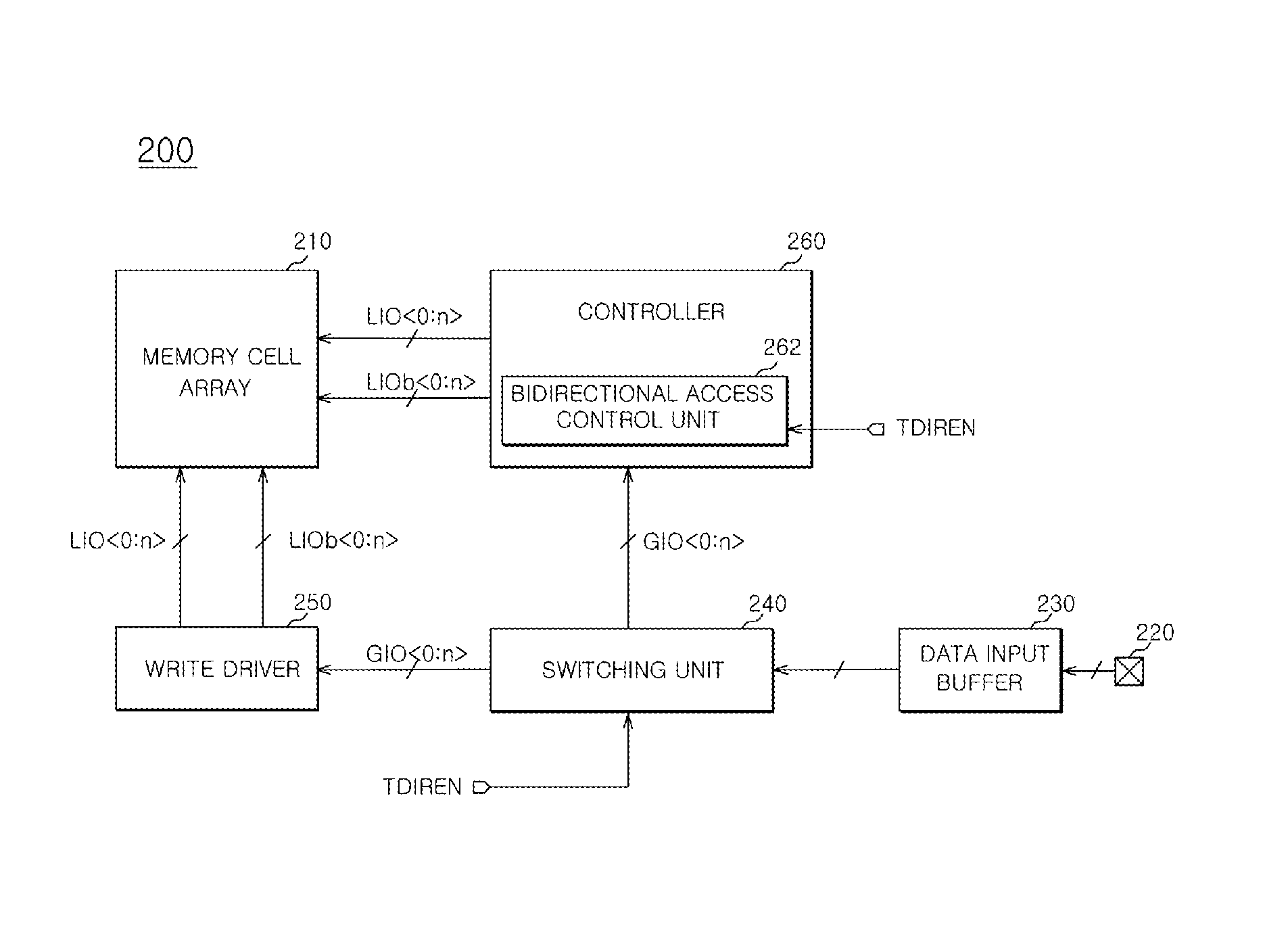
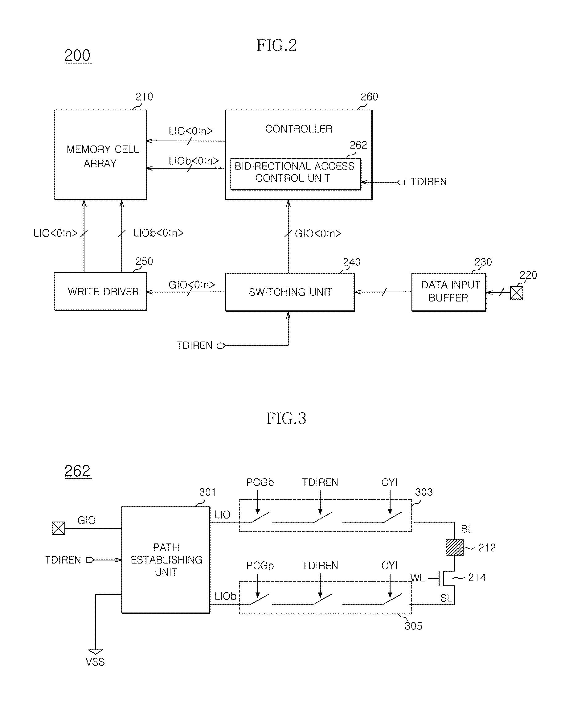
[0026]FIG. 2 is a configuration diagram of a semiconductor memory apparatus in accordance with an exemplary embodiment of the present invention.

[0027]FIG. 2 shows main components of a semiconductor memory apparatus for convenience of explanation. However, it is apparent to those skilled in the art that the semiconductor memory apparatus may include other components necessary for operating the semiconductor memory apparatus, for example, an address processing circuit, a control signal generation circuit, or the like.

[0028]Referring to FIG. 2, a semiconductor memory apparatus 200 according to an embodiment of the present invention may include a memory cell array 210, data input and output pads 220 (e.g., DQ pads), a data input buffer 230, a switching unit 240, a write driver ...


PUM


Abstract

Disclosed is a semiconductor memory apparatus, including: a memory cell array configured to include a plurality of memory cells; a switching unit configured to be coupled to data input and output pads and control a data transfer path of data applied to the data input and output pads in response to a test mode signal; a write driver configured to drive data transferred from the switching unit and write the data in the memory cell array at a normal mode; and a controller configured to transfer the data from the switching unit to the memory cell at a test mode.

Description

CROSS-REFERENCES TO RELATED APPLICATION[0001]The present application claims priority under 35 U.S.C. §119(a) to Korean application number 10-2011-0114430, filed on Nov. 4, 2011, in the Korean Intellectual Property Office, which is incorporated herein by reference in its entirety.BACKGROUND[0002]1. Technical Field[0003]Exemplary embodiments relate generally to a semiconductor integrated circuit, and more particularly to a semiconductor memory apparatus and a test circuit therefor.[0004]2. Related Art[0005]Generally, when data are written in a memory cell of a semiconductor memory apparatus, the data input through input / output pads are written into cells by a write driver. Further, when data are read from memory cells, the data in the memory cells are transferred to a sense amplifier, output amplified data through the input / output pads.[0006]FIG. 1 is a configuration diagram of a general semiconductor memory apparatus.[0007]As shown in FIG. 1, a semiconductor memory apparatus 100 incl...

Claims


Application Information

Patent Timeline
Patent Type & Authority Patents(United States)
IPC IPC(8): G11C11/00G11C29/48G11C29/12
CPCG11C29/1201G11C29/48G11C29/00
Inventor LEE, JAE, UNG
Owner SK HYNIX INC
Why Eureka
Try Eureka