Finger sensing device including differential measurement circuitry and related methods

a technology of differential measurement and finger sensing, applied in the field of electronic devices, can solve the problems of affecting the image quality of sliding sensors, the silicon space of smaller components may be unused, and the fingerprint sensor cannot be made smaller than, so as to achieve the effect of reducing nois

Active Publication Date: 2014-11-18
APPLE INC
View PDF36 Cites 54 Cited by
  • Summary
  • Abstract
  • Description
  • Claims
  • Application Information

AI Technical Summary

Benefits of technology

[0014]In view of the foregoing background, it is therefore an object of the present invention to provide a finger sensing device that can generate a reduced noise finger image from a finger positioned at a relatively large distance from the array of finger sensing pixels.
[0015]This and other objects, features, and advantages in accordance with the present invention are provided by a finger sensing device that may include an array of finger sensing pixels to receive a user's finger adjacent thereto. Each finger sensing pixel may include a finger sensing electrode. The finger sensing device may include a finger drive electrode configured to couple a drive signal through the user's finger to the array of finger sensing pixels and differential pixel measurement circuitry coupled to the array of finger sensing pixels and configured to generate a plurality of interpixel difference measurements for adjacent pairs of the finger sensing pixels. Accordingly, the finger sensing device may generate a reduced noise finger image from a finger positioned at a relatively large distance from the array of finger sensing pixels.

Problems solved by technology

Electronic fingerprint sensors, however, generally cannot be made smaller than the area of the finger skin that needs to be imaged.
One of the only results of smaller component geometries may be unused silicon space under the sensor pixels.
Yet, the sliding sensors may be subject to significant image distortion, and / or they may provide an inconvenient user paradigm.
Image distortion or noise may also be present when it may be desirable to sense a finger image from fingers positioned at a relatively greater distance away from an array of finger sensing pixels.
The need for close proximity to the user's finger typically makes the mechanical packaging and the integration of these devices into their host products more difficult and more costly.
Specialized packaging increases the cost of these sensors.
The need for the user's finger to be close to the array of finger sensing pixels may limit the thickness of the material that can be placed over that array, which may increasingly restrict the use of both protective and cosmetic coatings over the array area.
However, a negative aspect of these mounting arrangements may include increased difficulty and cost to seal the opening for the finger sensor in the host device case against the ingress of moisture, dust, and other contaminants.
Additionally, the opening in the case with the finger sensor protruding may be cosmetically unacceptable to the intended appearance of the host device, and mounting the finger sensor in an opening in the case may be difficult and costly in some devices.

Method used


Image

  • Finger sensing device including differential measurement circuitry and related methods
  • Finger sensing device including differential measurement circuitry and related methods
  • Finger sensing device including differential measurement circuitry and related methods

Examples


Embodiment Construction

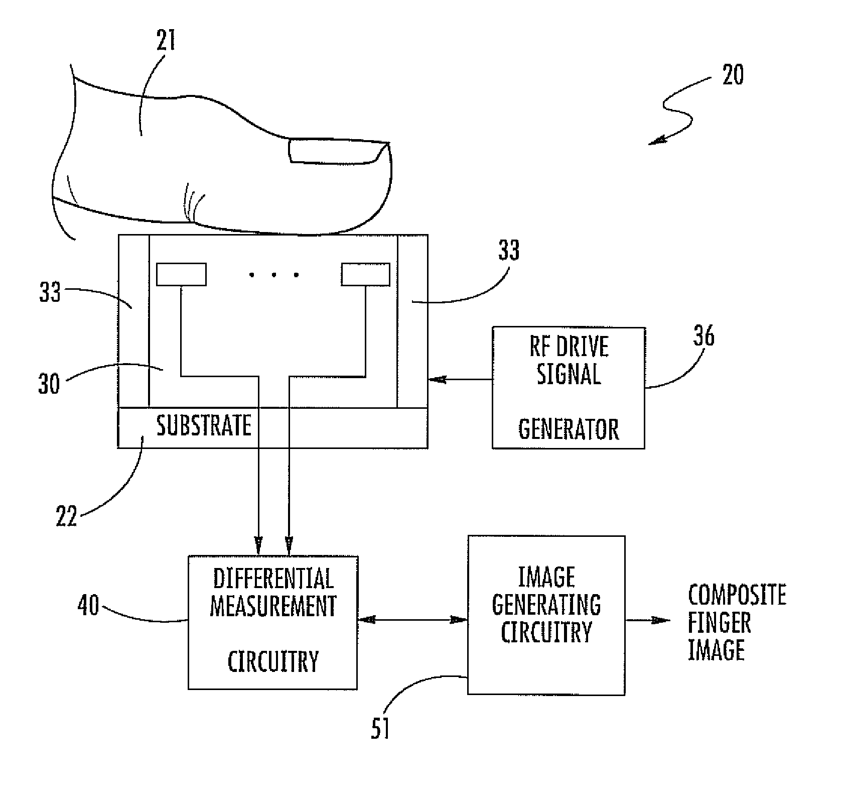
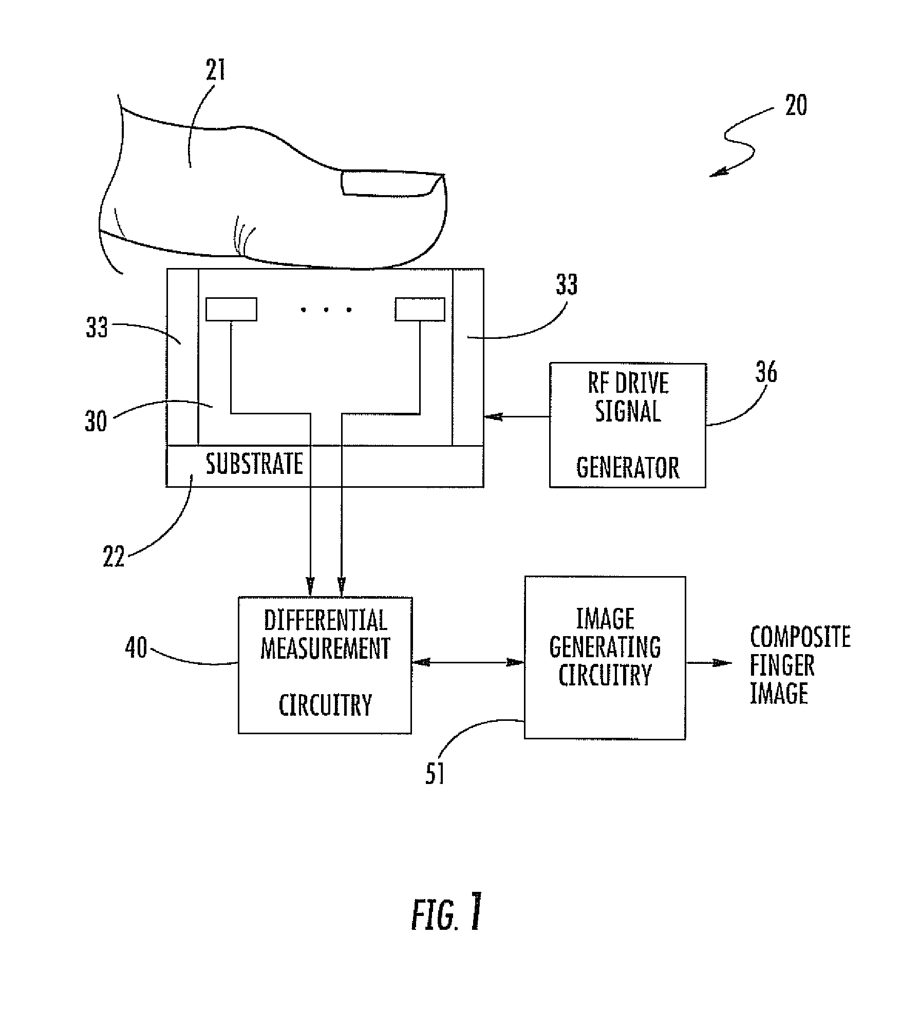
[0038]The present invention will now be described more fully hereinafter with reference to the accompanying drawings, in which preferred embodiments of the invention are shown. This invention may, however, be embodied in many different forms and should not be construed as limited to the embodiments set forth herein. Rather, these embodiments are provided so that this disclosure will be thorough and complete, and will fully convey the scope of the invention to those skilled in the art. Like numbers refer to like elements throughout, and prime and multiple prime notation is used to indicate similar elements in alternative embodiments.

[0039]Referring initially to FIG. 1, a finger sensing device 20 includes an array of finger sensing pixels 30 to receive a user's finger 21 adjacent thereto. The array of finger sensing pixels 30 is carried by a semiconductor substrate 22. The array of finger sensing pixels 30 may be any array size, as will be appreciated by those skilled in the art. Each...


PUM


Abstract

A finger sensing device may include an array of finger sensing pixels to receive a user's finger adjacent thereto. Each finger sensing pixel may include a finger sensing electrode. The finger sensing device may include a finger drive electrode configured to couple a drive signal through the user's finger to the array of finger sensing pixels. The finger sensing device may also include differential pixel measurement circuitry coupled to the array of finger sensing pixels and configured to generate a plurality of interpixel difference measurements for adjacent pairs of the finger sensing pixels.

Description

RELATED APPLICATION[0001]The present application is based upon previously filed copending provisional application Ser. No. 61 / 391,327, filed Oct. 8, 2010, the entire subject matter of which is incorporated by reference in its entirety.FIELD OF THE INVENTION[0002]The present invention relates to the field of electronics, and, more particularly, to finger sensing devices and related methods.BACKGROUND OF THE INVENTION[0003]Fingerprint sensing and matching is a reliable and widely used technique for personal identification or verification. In particular, a common approach to fingerprint identification involves scanning a sample fingerprint or an image thereof and storing the image and / or unique characteristics of the fingerprint image. The characteristics of a sample fingerprint may be compared to information for reference fingerprints already in a database to determine proper identification of a person, such as for verification purposes.[0004]In recent years it has been practical and ...

Claims


Application Information

Patent Timeline
Patent Type & Authority Patents(United States)
IPC IPC(8): G06K9/60G06K9/00G06K7/08G06V10/20
CPCG06K9/0002G06K9/605G06V40/1306G06V10/20G06V10/40G06F18/00
Inventor SETLAK, DALE R.LANDY, PATRICK J.STRAUB, ALBERT M.SCHENK, ROGER LEE
Owner APPLE INC
Why Eureka
Try Eureka