Method for manufacturing chip package structure

a technology of chip and package structure, which is applied in the direction of electrical equipment, semiconductor devices, semiconductor/solid-state device details, etc., can solve the problems of difficult alignment between solder bumps and pads, inability to meet the requirement of fine-pitch, and prone to smaller pads. to achieve the effect of precise alignmen

Active Publication Date: 2014-11-25
CHIPMOS TECH INC
View PDF9 Cites 0 Cited by
  • Summary
  • Abstract
  • Description
  • Claims
  • Application Information

AI Technical Summary

Benefits of technology

[0009]The invention is directed to a method for manufacturing a chip package structure. The method not only achieves precise alignment between solder materials and pads but also prevents bridge effects and short-circuit conditions from occurring when the solder materials undergo a reflow process.
[0010]The invention is further directed to a method for manufacturing a chip package structure. The method allows a redistribution layer to be formed when pads are formed, so as to simplify the entire manufacturing process and improve production efficiency.
[0013]According to the method for manufacturing the chip package structure described above, the patterned photoresist layer is removed after the chip is connected to the connection terminals of the carrier through the connection conductors. Thereby, precise alignment between the connection conductors and the connection terminals can be achieved, and the bridge of solder materials and the resultant short-circuit defect may be better prevented when the connection conductors and the connection terminals are connected. Additionally, in the method for manufacturing the chip package structure, the connection terminals may be formed together with the wiring pattern that is connected to the connection terminals, so as to rearrange the electrical contact points of the connection terminals. Thereby, the number of times of forming the redistribution layer subsequently may be reduced. As a result, the manufacturing costs may be lowered down, and the yield and the efficiency of the manufacturing process can be ameliorated.

Problems solved by technology

Due to the limited space in the circuit board, pitches among the pads are prone to become smaller and smaller.
This is detrimental to the printing or placement of large solder bumps; what is more, alignment between the solder bumps and the pads becomes more difficult.
Since the pads are arranged on the surface of the substrate in a fine-pitch manner, bridge effects and short-circuit conditions may occur when the solder bumps are in the melted state during the reflow process; thereby, the requirement of fine-pitch cannot be satisfied.

Method used


Image

  • Method for manufacturing chip package structure
  • Method for manufacturing chip package structure
  • Method for manufacturing chip package structure

Examples


Embodiment Construction

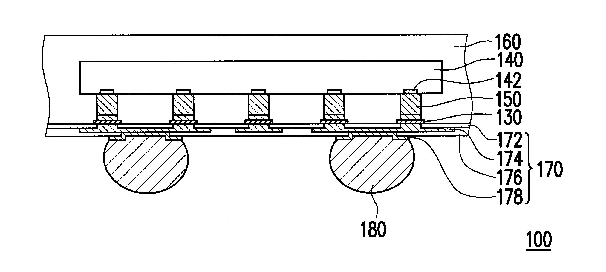
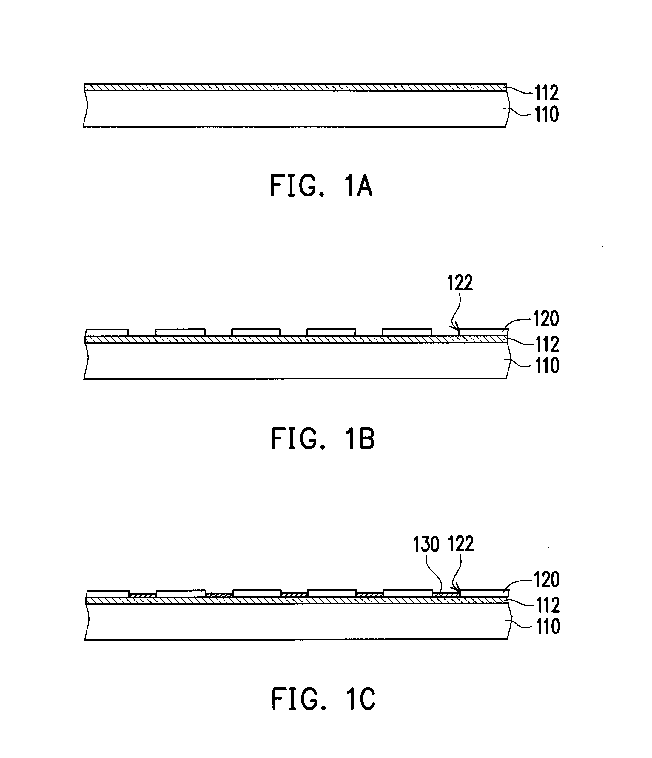
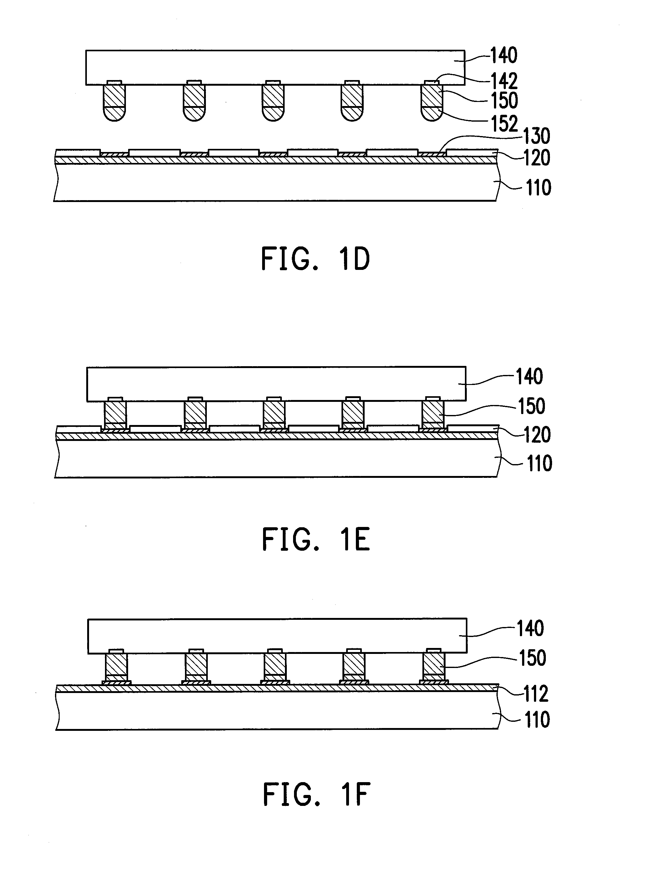
[0020]FIG. 1A to FIG. 1J are schematic cross-sectional flowcharts illustrating a method for manufacturing a chip package structure according to an embodiment of the invention. With reference to FIG. 1A and FIG. 1B, in the present embodiment, the method for manufacturing a chip package structure includes following steps. A carrier 110 is provided, and the carrier 110 has a metal layer 112. A patterned photoresist layer 120 is formed on the metal layer 112. As shown in FIG. 1B, the patterned photoresist layer 120 has a plurality of first openings 122 exposing a portion of the metal layer 112. With reference to FIG. 1C, connection terminals 130 are formed in the first openings 122, respectively, and the connection terminals 130 are connected to the metal layer 112. With reference to FIG. 1D and FIG. 1E, a chip 140 is placed on the carrier 110, and first pads 142 of the chip 140 are respectively connected to the connection terminals 130 through a plurality of connection conductors 150. ...


PUM


Abstract

A method for manufacturing a chip package structure includes following steps. A carrier having a metal layer is provided. A patterned photoresist layer is formed on the metal layer. The patterned photoresist layer has a plurality of first openings exposing a portion of the metal layer. Connection terminals are formed in the first openings, respectively, and the connection terminals are connected to the metal layer. A chip is placed on the carrier, and first pads of the chip are respectively connected to the connection terminals through a plurality of connection conductors. After the chip is placed on the carrier, the patterned photoresist layer is removed. A encapsulant is formed on the carrier. The encapsulant encapsulates the chip, the connection conductors, and the metal layer. The carrier and the metal layer are removed to expose the connection terminals.

Description

CROSS-REFERENCE TO RELATED APPLICATION[0001]This application claims the priority benefit of Taiwan application serial no. 102114827, filed on Apr. 25, 2013. The entirety of the above-mentioned patent application is hereby incorporated by reference herein and made a part of this specification.BACKGROUND OF THE INVENTION[0002]1. Field of the Invention[0003]The invention relates to a method for manufacturing a package structure; more particularly, the invention relates to a method for manufacturing a chip package structure.[0004]2. Description of Related Art[0005]In recent years, with rapid progress of electronic technologies and advancement of high-tech electronic industry, human-oriented electronic products with superior performance have brought forth a new era and have been designed to cater to the trend of being light, thin, short, and small. Owing to said trend, circuit boards with fine pitch wires, compactness, and favorable performance have become one of the main media for holdi...

Claims


Application Information

Patent Timeline
Patent Type & Authority Patents(United States)
IPC IPC(8): H01L21/44H01L21/56H01L23/00
CPCH01L24/83H01L21/561H01L24/81H01L21/568H01L24/03H01L24/05H01L24/13H01L24/19H01L24/96H01L2224/03003H01L2224/03334H01L2224/0345H01L2224/0346H01L2224/0401H01L2224/04105H01L2224/05005H01L2224/05008H01L2224/05569H01L2224/05572H01L2224/12105H01L2224/131H01L2924/00014H01L2224/13H01L2924/014
Inventor WANG, CHIEN-HAO
Owner CHIPMOS TECH INC
Why Eureka
Try Eureka