
Channel hot carrier tolerant tracking circuit for signal development on a memory SRAM

Active Publication Date: 2015-01-27
TEXAS INSTR INC
View PDF6 Cites 5 Cited by
  • Summary
  • Abstract
  • Description
  • Claims
  • Application Information

AI Technical Summary

Benefits of technology

The patent describes a method and circuit for reducing degradation in transistors used in tracking circuits of memory devices. By dividing the number of times a tracking circuit is accessed by the number of memory cells in the array, degradation in the transistors is reduced. This results in a reduction in read failures and increased data output timing paths. The circuit also includes a delay line circuit and a dummy word line circuit to determine the signal develop time of a memory cell. Overall, the invention improves the reliability and performance of memory devices.

Problems solved by technology

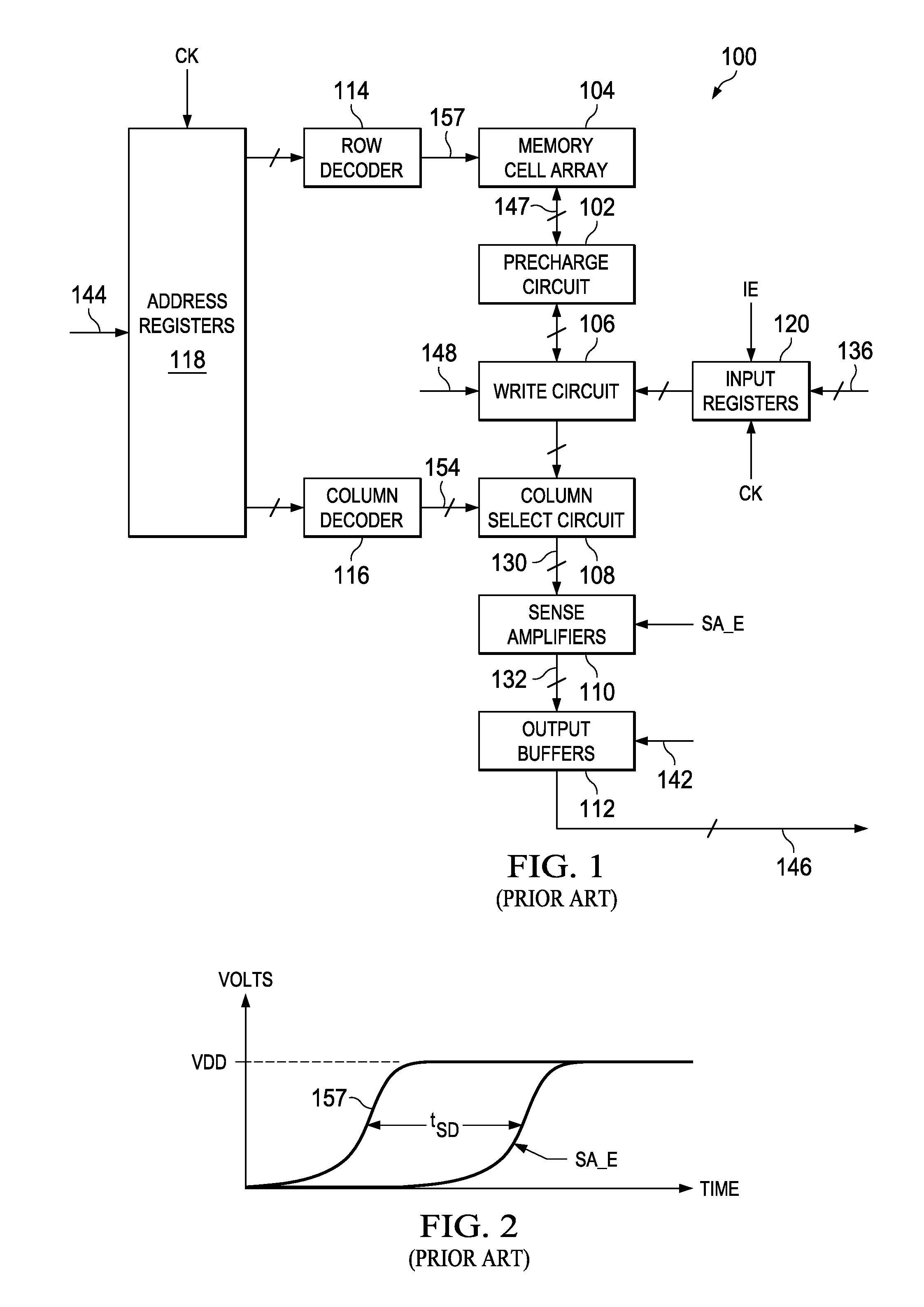
Because the transistors in the tracking circuits can be activated each time a memory array is read, the transistors may degrade faster than the transistors in the memory array.
This degradation in the transistors in the tracking circuits can cause changes in the time allowed for signal development on bit lines of the memory array.
Changes in the time allowed for signal development can cause a read of the memory array to fail or cause the read access time to increase leading to timing violations in the data output timing paths.

Method used


Image

  • Channel hot carrier tolerant tracking circuit for signal development on a memory SRAM
  • Channel hot carrier tolerant tracking circuit for signal development on a memory SRAM
  • Channel hot carrier tolerant tracking circuit for signal development on a memory SRAM

Examples


Embodiment Construction

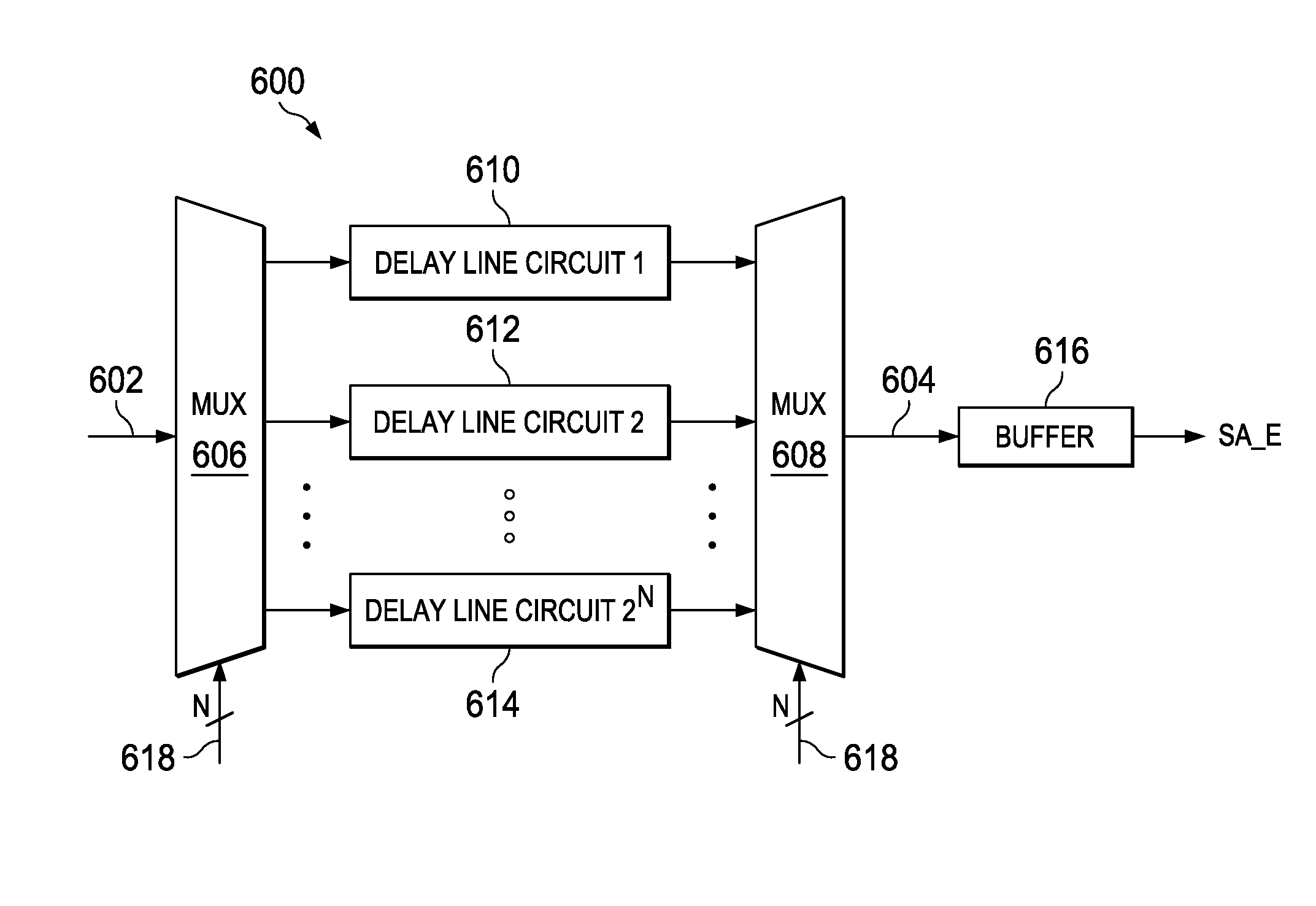
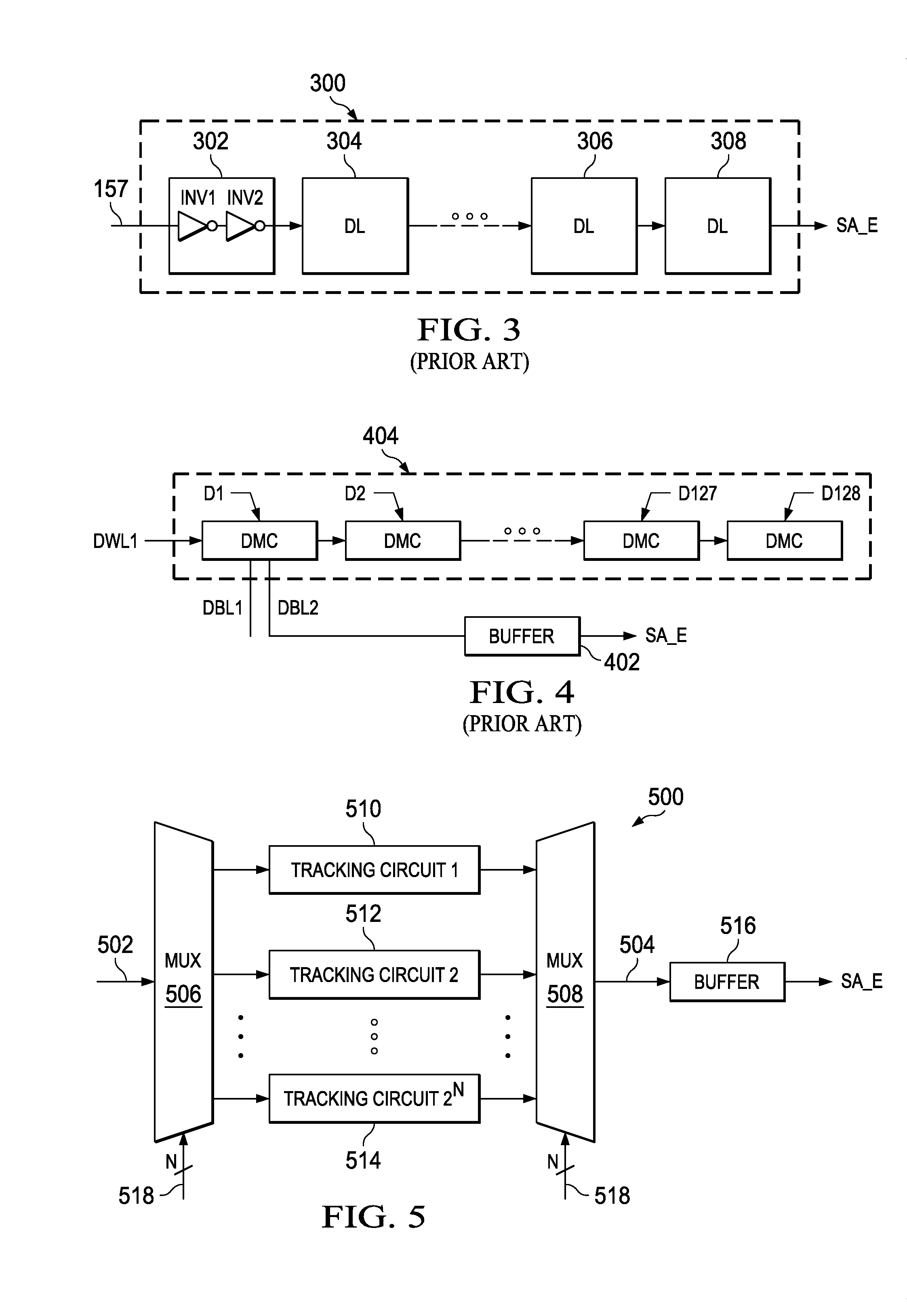
[0013]The drawings and description, in general, disclose a method and an electrical circuit for reducing degradation in the NMOS (n-type metal oxide semiconductor) transistors used in tracking circuits. A tracking circuit creates a timing delay from the time a dummy word line is activated to the time a sense amp in a memory array is activated. In an embodiment of the invention, degradation in the NMOS transistors used in tracking circuits is reduced by dividing the number of times a single tracking circuit is accessed by the number of tracking circuits.

[0014]In an embodiment of the invention, the number of tracking circuits is equal to 2N where N is equal to the least significant bits of the row address that is used to address an SRAM array. Each time the SRAM array is read, one of the 2N tracking circuits is enabled depending on the N least significant bits of the row address. As a result, the degradation of the tracking circuits is reduced by a factor of 2N on average.

[0015]FIG. 1...


PUM


Abstract

An embodiment of the invention discloses an electronic device for reducing degradation in NMOS circuits in a tracking circuit. A first multiplexer selects, based on N bits from a row address in a memory array, which tracking circuit from a group of 2N tracking circuits will be used to provide a signal develop time for a memory cell in the memory array using a dummy word line signal. A second multiplexer selects, based on the N bits from the row address for a memory array, which output from the tracking circuits is used to enable the sense amp enable signal.

Description

[0001]This application for patent claims priority to U.S. Provisional Application No. 61 / 703,623 entitled “Channel Hot Carrier Tolerant Tracking Circuit for Signal Development on an SRAM” filed Sep. 20, 2012, which is incorporated by reference herein.BACKGROUND[0002]This invention relates to integrated circuits, particularly to memory devices, in either embedded form or stand alone (i.e. discrete) form.[0003]Memory cells in devices, for example static random access memory (SRAM) store logical binary values (i.e. either a logical one or a logical zero). When a memory cell is selected by a word line during a read, the voltage on a latch in the memory cell begins to change the voltages on the bit lines attached to the memory cell (i.e. signal is developing on the bit lines). Because the signal on the bit lines is initially small, a certain amount of time must pass to allow the signal on the bit lines to grow larger. When the signal on the bit lines reaches a certain value, this value m...

Claims


Application Information

Patent Timeline
IPC IPC(8): G11C7/10
CPCG11C7/08G11C7/222G11C7/227G11C8/18G11C11/418
Inventor SRIDHARA, SRINIVASA
Owner TEXAS INSTR INC
Learn More