High frequency monolithic microwave integrated circuit connection

a monolithic microwave and integrated circuit technology, applied in the direction of electrical apparatus, semiconductor devices, semiconductor/solid-state device details, etc., can solve the problems of less mechanical yield, less electrical yield, and difficulty in external compensation, so as to facilitate automated bonding techniques, reduce the size of radio frequency pads, and ensure the effect of electrical yield

Inactive Publication Date: 2015-03-03
MACOM TECH SOLUTIONS HLDG INC
View PDF3 Cites 9 Cited by
  • Summary
  • Abstract
  • Description
  • Claims
  • Application Information

AI Technical Summary

Benefits of technology

[0005]The objects, features and advantages of the present invention include providing a high frequency monolithic microwave integrated circuit connection that may (i) reduce a radio frequency pad size compared with conventional designs, (ii) have sufficient surface area on the radio frequency pad to facilitate automated bonding techniques, (iii) include a chamfered region, (iv) implement an irregular hexagonal shape, (v) support E band frequencies, (vi) provide on-chip compensation for radio frequency signals and / or (vii) be, implemented on an integrated circuit.

Problems solved by technology

However, sharp angles in the traces degrade the performance as the frequency increases and so external compensation becomes more difficult.
Furthermore, mechanical yields are lower in manual and automated assembly factory environments with the smaller pads which lead to lower electrical yields.

Method used


Image

  • High frequency monolithic microwave integrated circuit connection
  • High frequency monolithic microwave integrated circuit connection
  • High frequency monolithic microwave integrated circuit connection

Examples


Embodiment Construction

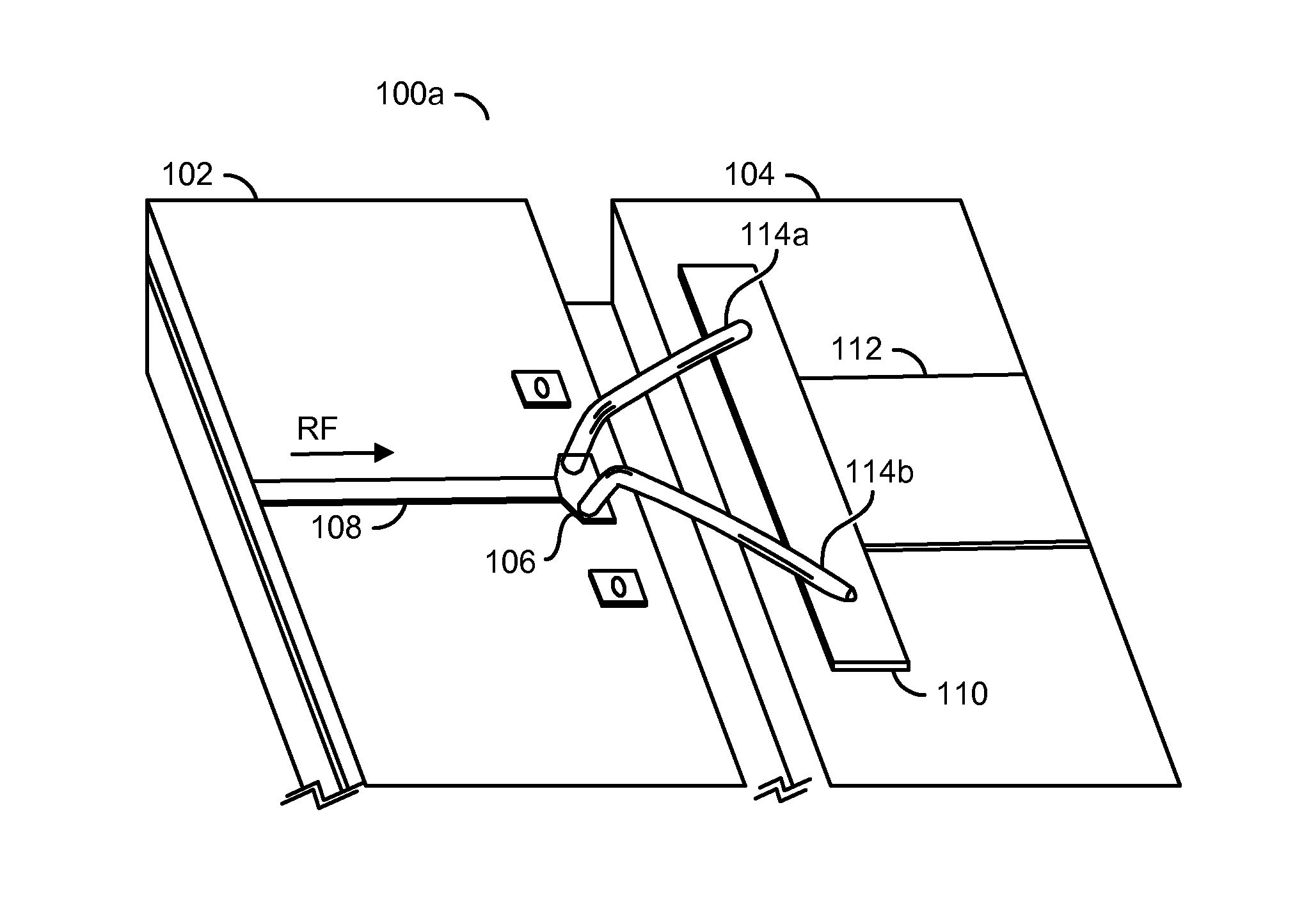
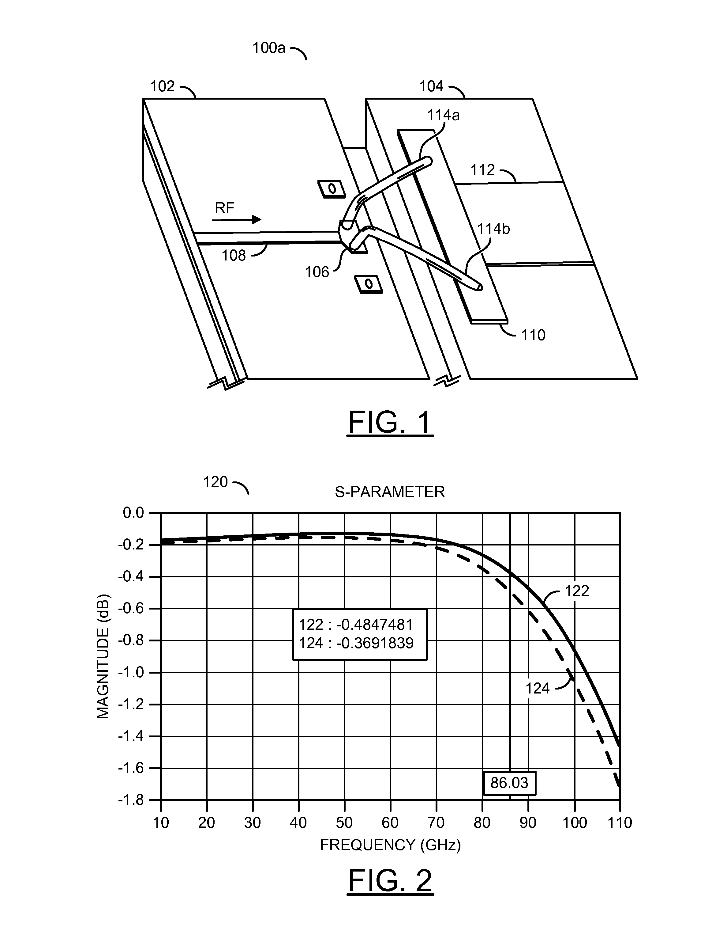
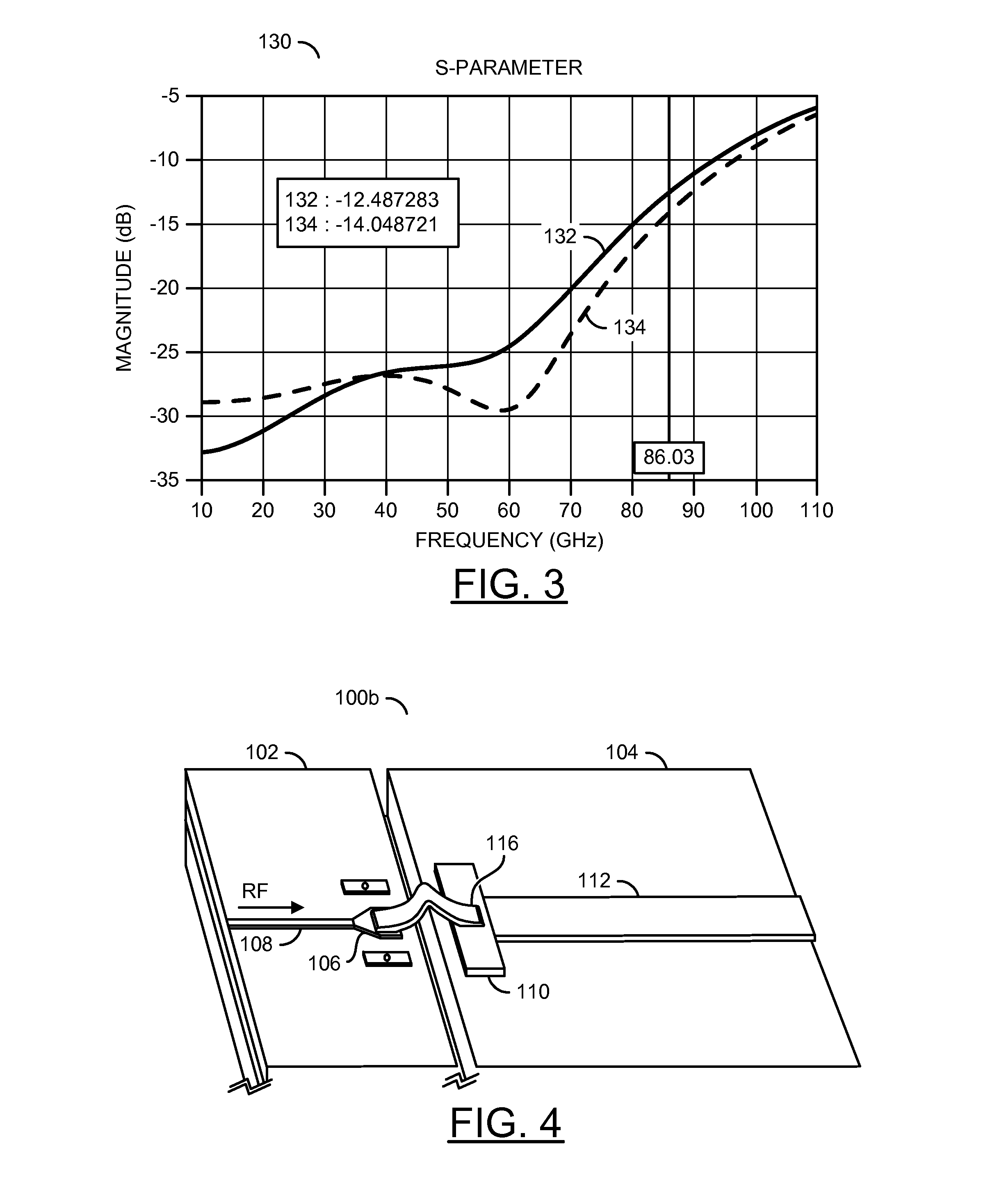
[0024]Some embodiments of the present invention generally provide a bonding pad design that supports signals in a radio frequency range (e.g., less than approximately 300 gigahertz-GHz), microwave frequency range (e.g., super-high frequency to extremely high frequency bands of approximately 3 GHz to approximately 300 GHz), a V band (e.g., approximately 50 GHz to approximately 75 GHz), an E band (e.g., approximately 60 GHz to approximately 90 GHz) and / or in a range of approximately 10 GHz to 300 GHz. In some embodiments, the bonding pads generally have an irregular hexagonal (or 6-sided) shape that is tapered to match a corresponding transmission line. The 6 sides may be see as viewed in a plane parallel to a top surface of the circuit 102. The bonding pads include a bond region having sufficient area to reliably accept bonding wires and / or a bonding tape in an automated or manual bonding process. The tapered shape may provide on-chip frequency compensation to account for the inducta...


PUM


Abstract

An apparatus having a bonding pad and a conductor is disclosed. The bonding pad may be formed in a conductive layer of an integrated circuit. The bonding pad generally has (i) a bond region, (ii) an interface edge sized to match a transmission line and (iii) a tapered region between the bond region and the interface edge. The interface edge may be narrower than the bond region. The tapered region generally has a non-rectangular shape that spans from the bond region to the interface edge. The conductor may be bonded to the bond region. The conductor is generally configured to exchange a signal with the bond region. The signal may be in a microwave frequency range.

Description

FIELD OF THE INVENTION[0001]The present invention relates to high frequency input / output die connections generally and, more particularly, to a method and / or apparatus for implementing a high frequency monolithic microwave integrated circuit connection.BACKGROUND OF THE INVENTION[0002]Conventional radio frequency (i.e., RF) bonding pads are rectangular and have reasonable performance. Making the radio frequency bonding pads smaller improves the performance at frequencies above 8 gigahertz. However, sharp angles in the traces degrade the performance as the frequency increases and so external compensation becomes more difficult. Furthermore, mechanical yields are lower in manual and automated assembly factory environments with the smaller pads which lead to lower electrical yields.[0003]It would be desirable to implement a high frequency monolithic microwave integrated circuit connection.SUMMARY OF THE INVENTION[0004]The present invention concerns an apparatus having a bonding pad and...

Claims


Application Information

Patent Timeline
Patent Type & Authority Patents(United States)
IPC IPC(8): H01L23/58H01L23/00
CPCH01L24/05H01L24/03H01L23/66H01L24/45H01L24/48H01L24/49H01L2223/6611H01L2223/6683H01L2224/04042H01L2224/05552H01L2224/05555H01L2224/45014H01L2224/45144H01L2224/48091H01L2224/48137H01L2224/48157H01L2224/48465H01L2224/48472H01L2224/49111H01L2224/49171H01L2924/10271H01L2924/10329H01L2924/1033H01L2924/10335H01L2924/1421H01L2924/1423H01L2924/30107H01L2224/45015H01L2924/00014H01L2924/20751H01L2924/20752H01L2924/00H01L2924/206
Inventor TARAZI, JABRASNYGG, LEIF GORAN MARTIN
Owner MACOM TECH SOLUTIONS HLDG INC
Why Eureka
Try Eureka