
Stress relieving second level interconnect structures and methods of making the same

a second-level interconnect and stress-relief technology, applied in the direction of printed element electric connection formation, sustainable manufacturing/processing, final product manufacturing, etc., can solve the problems of reducing cost options, reducing stress-relief within the current interconnect structure, and affecting the reliability of the interconnect structure, so as to improve the thermo-mechanical reliability without compromising cost, reworkability or electrical performance.

Inactive Publication Date: 2015-03-03
GEORGIA TECH RES CORP
View PDF10 Cites 5 Cited by
  • Summary
  • Abstract
  • Description
  • Claims
  • Application Information

AI Technical Summary

Benefits of technology

[0014]In some embodiments, the second pad is of a size sufficient to prevent wicking of the solder bump.

Problems solved by technology

These interconnect structures, however, face fundamental challenges as the trend towards three-dimensional ICs and silicon and glass-based low-TCE interposer packages with fine-pitch board level assembly gains momentum.
First, providing a means for stress-relief within the current interconnect structures can be costly.
Lower cost options, however, tend to induce tremendous TCE mismatch between low-TCE packages and PCBs.
Second, this mismatch subsequently creates fundamental limitations in scaling down the pitch size with traditional solder compositions.
Third, current underfill requirements prevent reworkability.

Method used


Image

  • Stress relieving second level interconnect structures and methods of making the same
  • Stress relieving second level interconnect structures and methods of making the same
  • Stress relieving second level interconnect structures and methods of making the same

Examples


Embodiment Construction

[0032]Referring now to the figures, wherein like reference numerals represent like parts throughout the several views, exemplary embodiments of the present invention will be described in detail. Throughout this description, various components can be identified as having specific values or parameters, however, these items are provided as exemplary embodiments. Indeed, the exemplary embodiments do not limit the various aspects and concepts of the present invention as many comparable parameters, sizes, ranges, and / or values can be implemented.

[0033]It should also be noted that, as used in the specification and the appended claims, the singular forms “a,”“an,” and “the” include plural references unless the context clearly dictates otherwise. For example, reference to a component is intended also to include composition of a plurality of components. References to a composition containing “a” constituent is intended to include other constituents in addition to the one named. Also, in descr...


PUM


Abstract

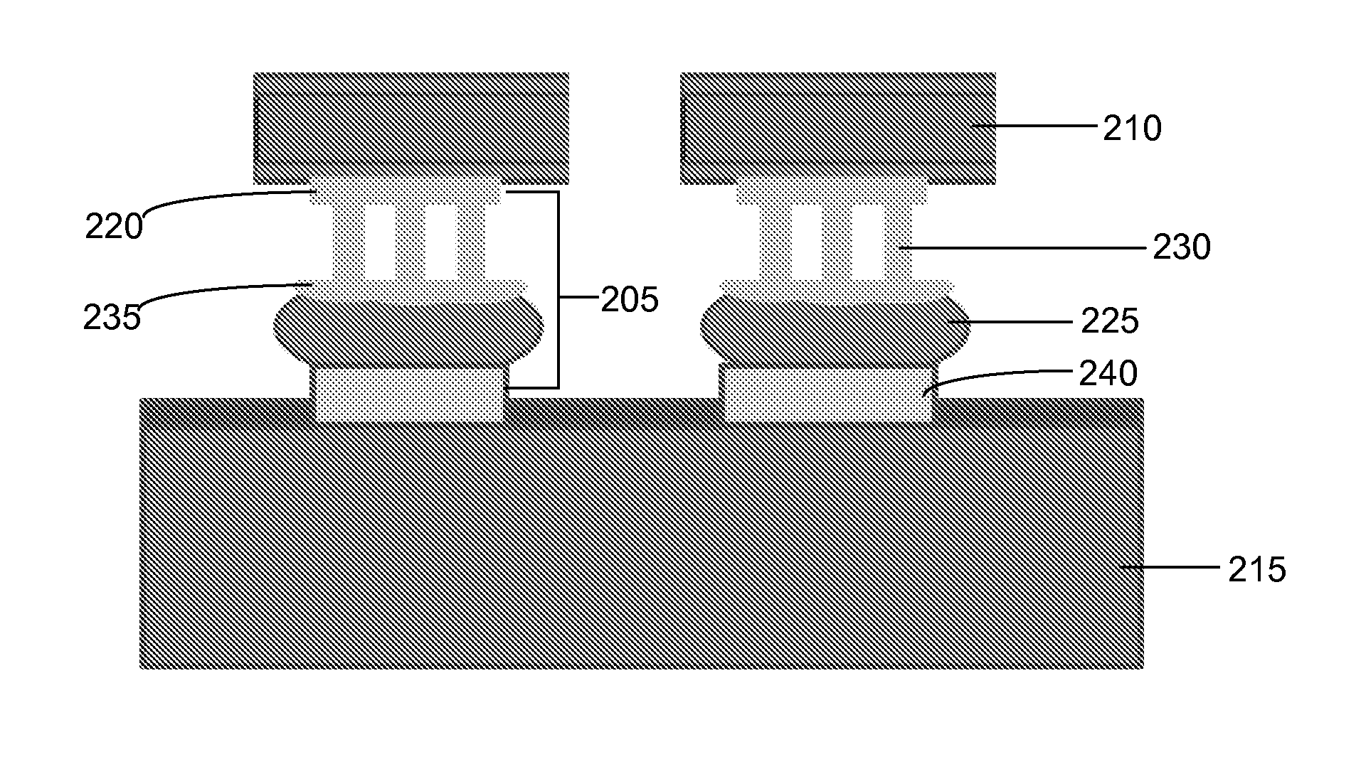
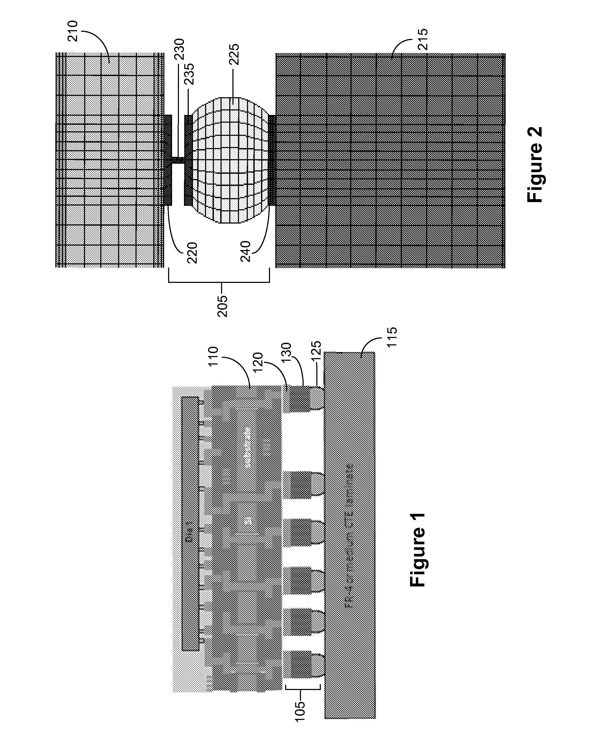
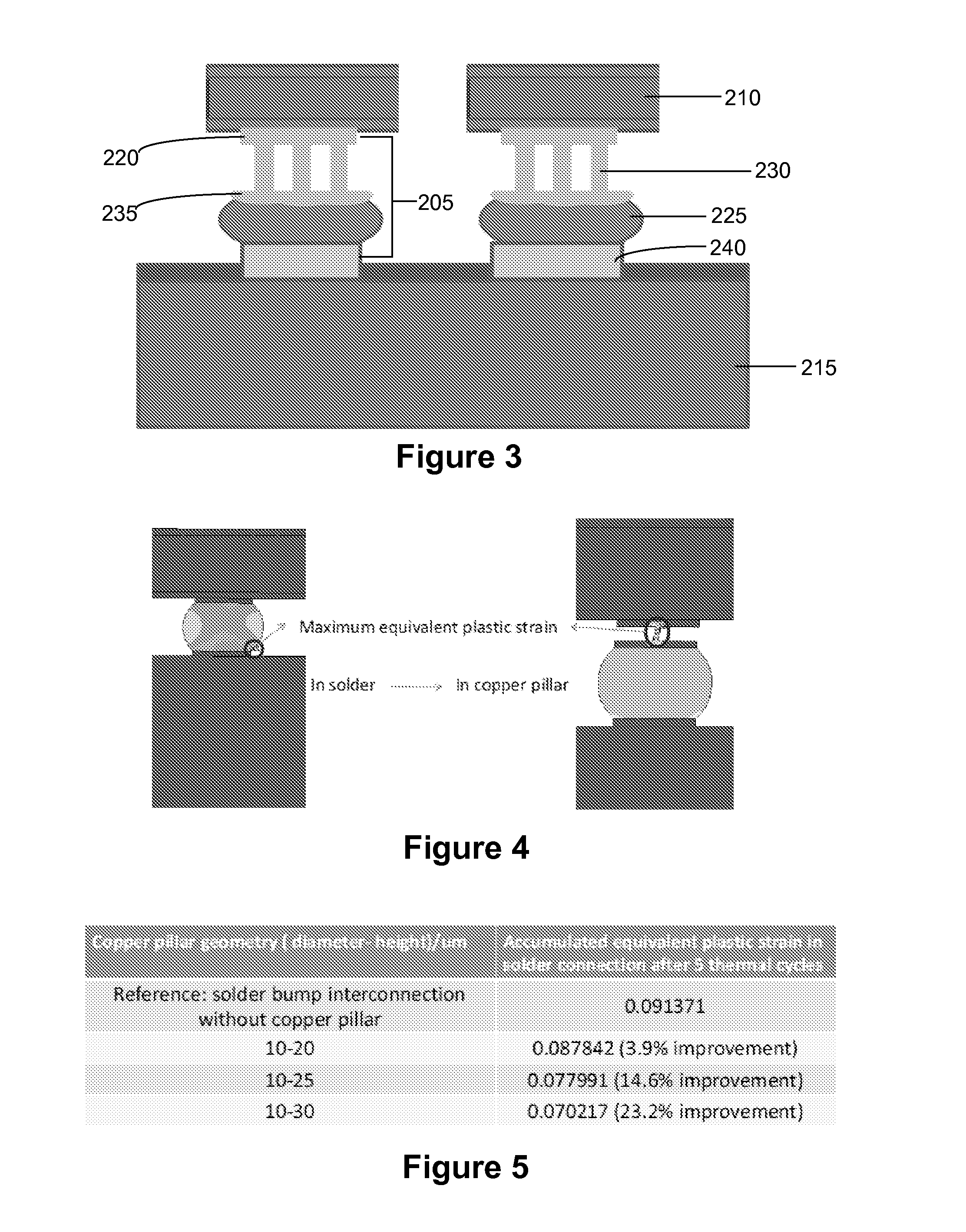
Provided is a stress-relieving, second-level interconnect structure that is low-cost and accommodates thermal coefficient of expansion (TCE) mismatch between low-TCE packages and printed circuit boards (PCBs). The interconnect structure comprises at least a first pad, a supporting pillar, and a solder bump, wherein the first pad and supporting pillar are operative to absorb substantially all plastic strain, thereby enhancing compliance between the two electronic components.

Description

CROSS-REFERENCE TO RELATED APPLICATIONS[0001]This application claims the benefit of International Patent Application Serial No. PCT / US2011 / 052384, filed 20 Sep. 2011, which claims the benefit of U.S. Provisional Patent Application Ser. No. 61 / 387,120, filed 28 Sep. 2010, and U.S. Provisional Patent Application Ser. No. 61 / 509,209, filed 19 Jul. 2011, which are incorporated herein by reference in their entirety as if fully set forth below.BACKGROUND[0002]1. Field[0003]The various embodiments of the present invention relate to second-level interconnect structures, wherein features of the interconnect structure may be altered to achieve desired fine-pitch and low-stress properties, and to methods of making and using the same.[0004]2. Description of Related Art[0005]Interconnects facilitate electrical communication between various electronic components within an electronic system. A “first-level” interconnect, for example, facilitates electrical communication between integrated circuits...

Claims


Application Information

Patent Timeline
Patent Type & Authority Patents(United States)
IPC IPC(8): H01L23/48H01L23/00H05K1/02H05K3/34H05K3/40
CPCH01L24/16H05K3/3436H05K3/4007H01L24/11H05K1/0271H01L2224/11472H01L2224/13011H01L2224/13017H01L2224/13078H01L2224/16225H01L2924/14H01L2924/181Y02P70/50H01L2924/00012H01L2924/00H01L23/48
Inventor RAJ, PULUGURTHA MARKONDEYAKUMBHAT, NITESHSUNDARAM, VENKATESH V.TUMMALA, RAO R.QIN, XIAN
Owner GEORGIA TECH RES CORP
Learn More