Method and circuit structure for suppressing single event transients or glitches in digital electronic circuits

a single event transient or glitch technology, applied in the field of single event transient or glitch suppressing in digital electronic circuits, can solve the problems of general sensitive to single event effects, affecting the state of the circuit, and affecting the effect of the circuit structure,

Active Publication Date: 2015-03-10
NELSON MANDELA METROPOLITAN UNIV
View PDF10 Cites 6 Cited by
  • Summary
  • Abstract
  • Description
  • Claims
  • Application Information

AI Technical Summary

Problems solved by technology

Unfortunately, while FPGAs offer several benefits for space-based electronics, they are generally sensitive to Single Event Effects (SEEs).
These deposited charges cause elevated local voltage levels in the circuit elements, which can non-destructively change the state of a bi-stable element.
However, when synchronous logic is disturbed by an SET on a clock edge, the temporarily incorrect logic value is latched into the register.
The changes can cause the software to perform unintended commands and thus cause the software to “crash”.
Configuration memory upsets are especially problematic because such upsets affect both the state and operation of the design.
Configuration upsets may perturb the routing resources and logic functions in a way that changes the operation of the circuit.
However, in FPGAs with volatile memories, in particular in SRAM based FPGAs, the major contributor of errors caused by SETs is due to configuration memory errors.
Most DMR solutions, however, are only generally able to detect SEUs but not mask or correct them.
The main disadvantage of TMR is the excessive area overhead.
The hardened design, with triplication of the combinational circuit and additional voting circuitry, can have between 4 and 7 times more area and power consumption than the original circuit, which limits its usage to reliability-critical applications.
Radiation tolerant FPGAs for space and military applications are available, but these tend to be orders of magnitude more expensive than their off-the-shelf counterparts.
While this method is effective in mitigating SEUs, the voters require a significant amount of additional circuitry and complexity, double modular redundancy is still required, and a small additional delay is introduced during the time in which the circuit is “frozen”.
Furthermore, configuration memory errors are identified by detecting that the circuit has remained frozen for more than a predetermined time period and then reconfiguring the configuration memory.
This wait time introduces much longer time delays in the case of configuration memory errors.

Method used


Image

  • Method and circuit structure for suppressing single event transients or glitches in digital electronic circuits
  • Method and circuit structure for suppressing single event transients or glitches in digital electronic circuits
  • Method and circuit structure for suppressing single event transients or glitches in digital electronic circuits

Examples


Embodiment Construction

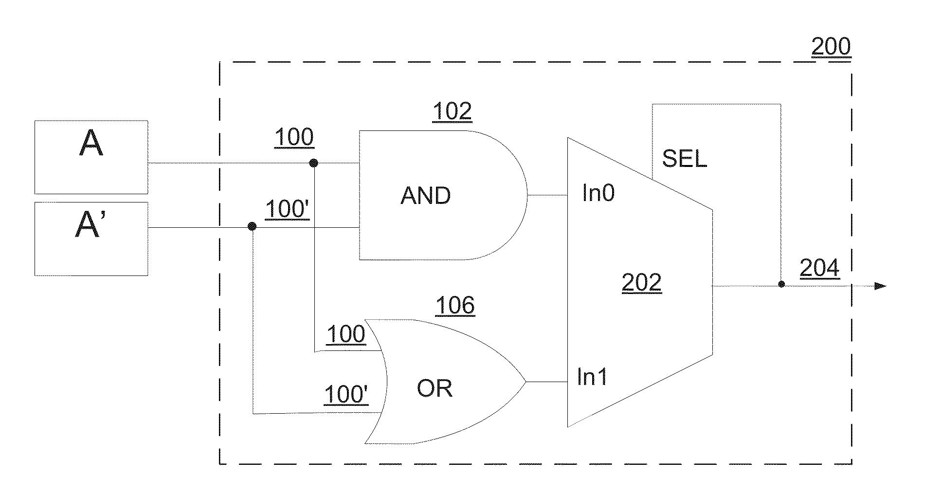
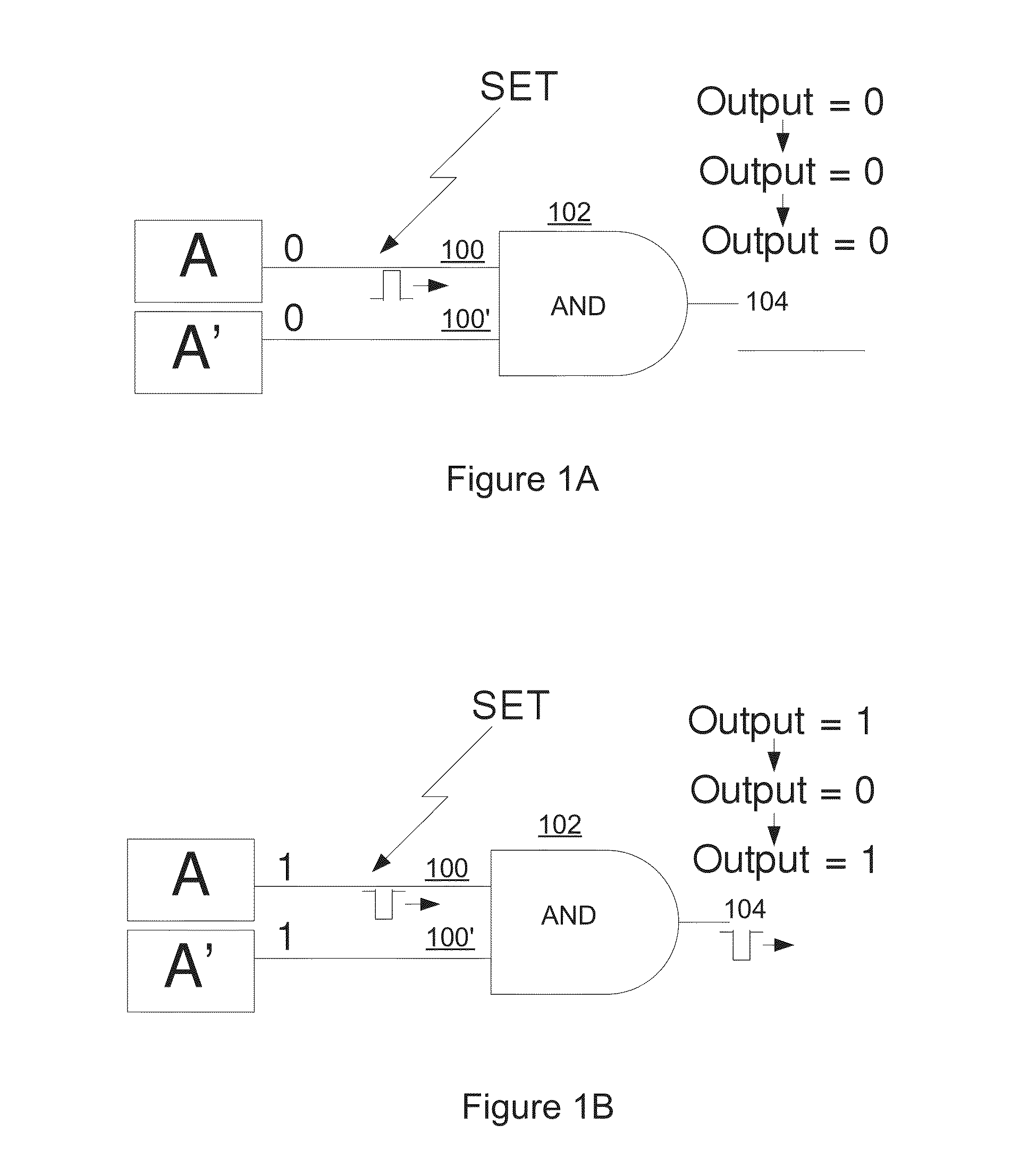
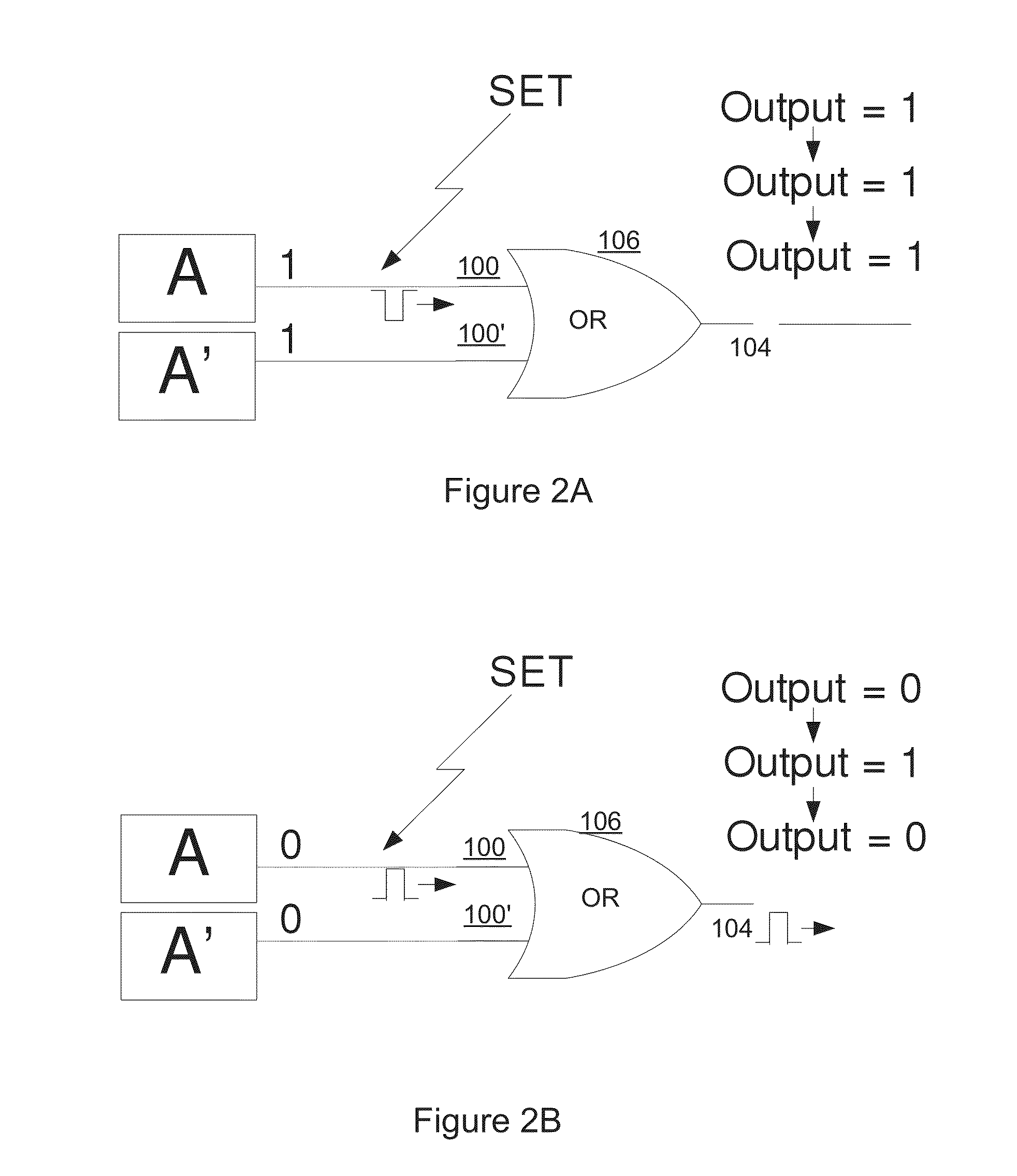
[0089]For a single event transient (SET) to result in a single event upset (SEU) in a digital electronic circuit such as a sequential circuit, three conditions have to be satisfied: (1) an active path must exist between the afflicted node and the output of the circuit; (2) the pulse must be wide enough to avoid inertial delay filtration through subsequent gates and survive electrical attenuation along the active path; and (3) the pulse should arrive within the setup and hold time of a latch element, such as a flip-flop, to be captured and cause a soft fault.

[0090]A sequential circuit operates by transitioning from one state to the next, generating different output signals. The part of a sequential circuit that is responsible for determining the next state is called the next-state-logic circuit, which is a combinational circuit. Based on the current state of the system (the state memory flip-flops) and any input signals, the next-state-logic combinational circuit will determine the n...


PUM


Abstract

A circuit structure (200) for suppressing single event transients (SETs) or glitches in digital electronic circuits is provided. The circuit structure includes a first input (100) which receives an output of a digital electronic circuit (A), a second input (100′) which receives a redundant or duplicated output of the digital electronic circuit (A′), and two sub-circuits (102, 106) that each receive the inputs and have one output. One of the sub-circuits is insensitive to a change in the value of one of its inputs when the inputs are in a first logic state and the other sub-circuit is insensitive to a change in the value of one of the inputs when the inputs are in a second, inverted logic state. The sub-circuit outputs are input into a two-input multiplexer (202) which has its output (204) connected to its selection port (SEL), and the sub-circuits are arranged so that the sub-circuit which is insensitive to a change in the value of one of its inputs is selected whenever the output of the multiplexer changes. The multiplexer output (204) is provided as a final output in which SETs and glitches have been suppressed.

Description

RELATED APPLICATIONS[0001]This application is a national phase filing of International Application No. PCT / IB2012 / 055738, filed Oct. 19, 2012, which claims priority to South African Application No. 2011 / 07718, filed Oct. 21, 2011; South African Application No. 2011 / 07719, filed Oct. 21, 2011; and South African Application No. 2012 / 00683, filed Jan. 27, 2012, the entire contents of all are incorporated by reference.FIELD OF THE INVENTION[0002]The invention relates to a method and circuit structure for suppressing single event transients or glitches in digital electronic circuits. The invention finds particular but by no means exclusive application in mitigating single event transients (SETs) in combinational circuits which form part of programmable sequential electronic circuits, such as volatile or non-volatile Field Programmable Gate Arrays (FPGAs) and Application Specific Integrated Circuits (ASICs).BACKGROUND TO THE INVENTION[0003]There is increasing interest in the use of field ...

Claims


Application Information

Patent Timeline
Patent Type & Authority Patents(United States)
IPC IPC(8): H03K19/003H03K19/00H03K19/007G01R31/3181
CPCH03K19/00346H03K19/0033H03K19/0008H03K19/0075G01R31/31816
Inventor SMITH, FAROUK
Owner NELSON MANDELA METROPOLITAN UNIV
Why Eureka
Try Eureka