

Manufacturing method for light-emitting device comprising multi-step cured silicon resin
Patent Information
- Authority / Receiving Office
- US · United States
- Patent Type
- Patents(United States)
- Current Assignee / Owner
- SHARP KK
- Publication Date
- 2015-04-14
- Estimated Expiration
- Not applicable · inactive patent
Smart Images
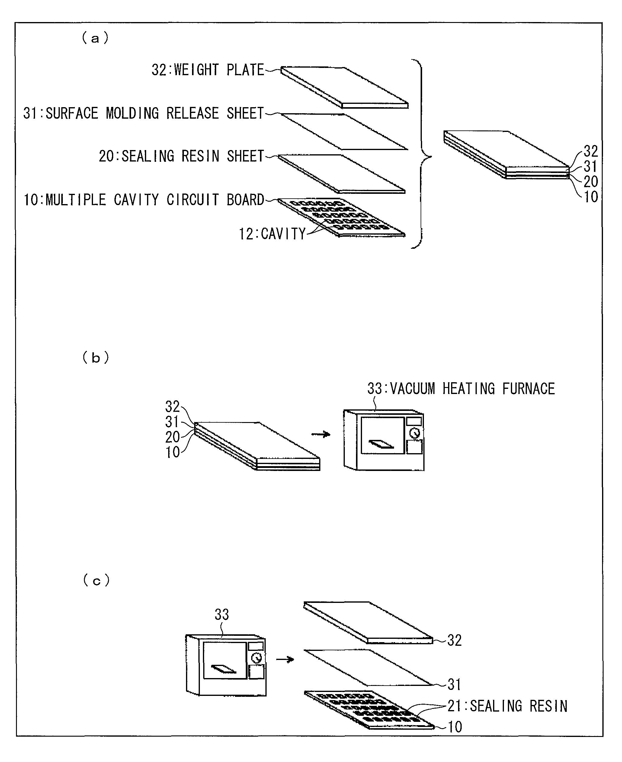
Figure 1 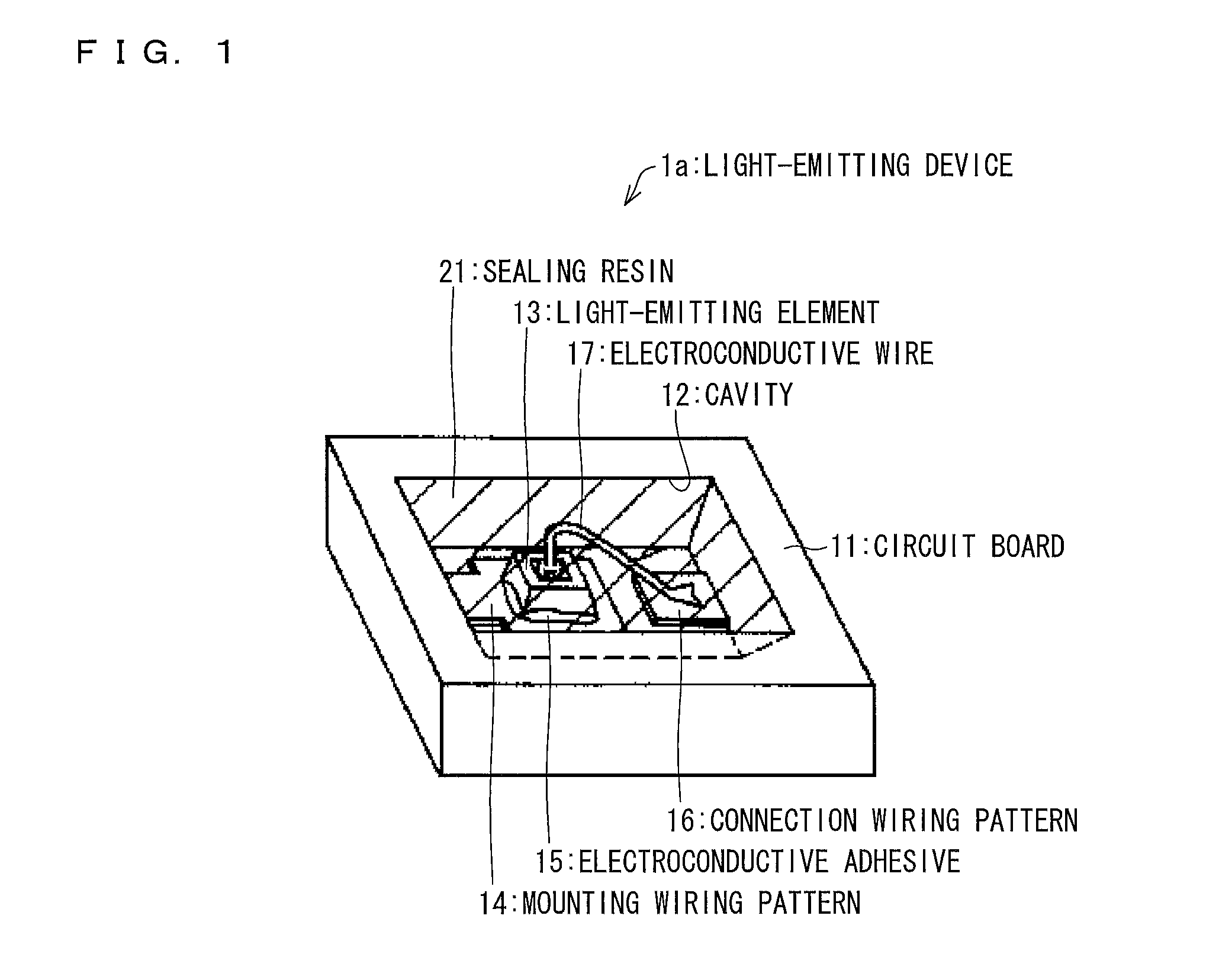
Figure 2 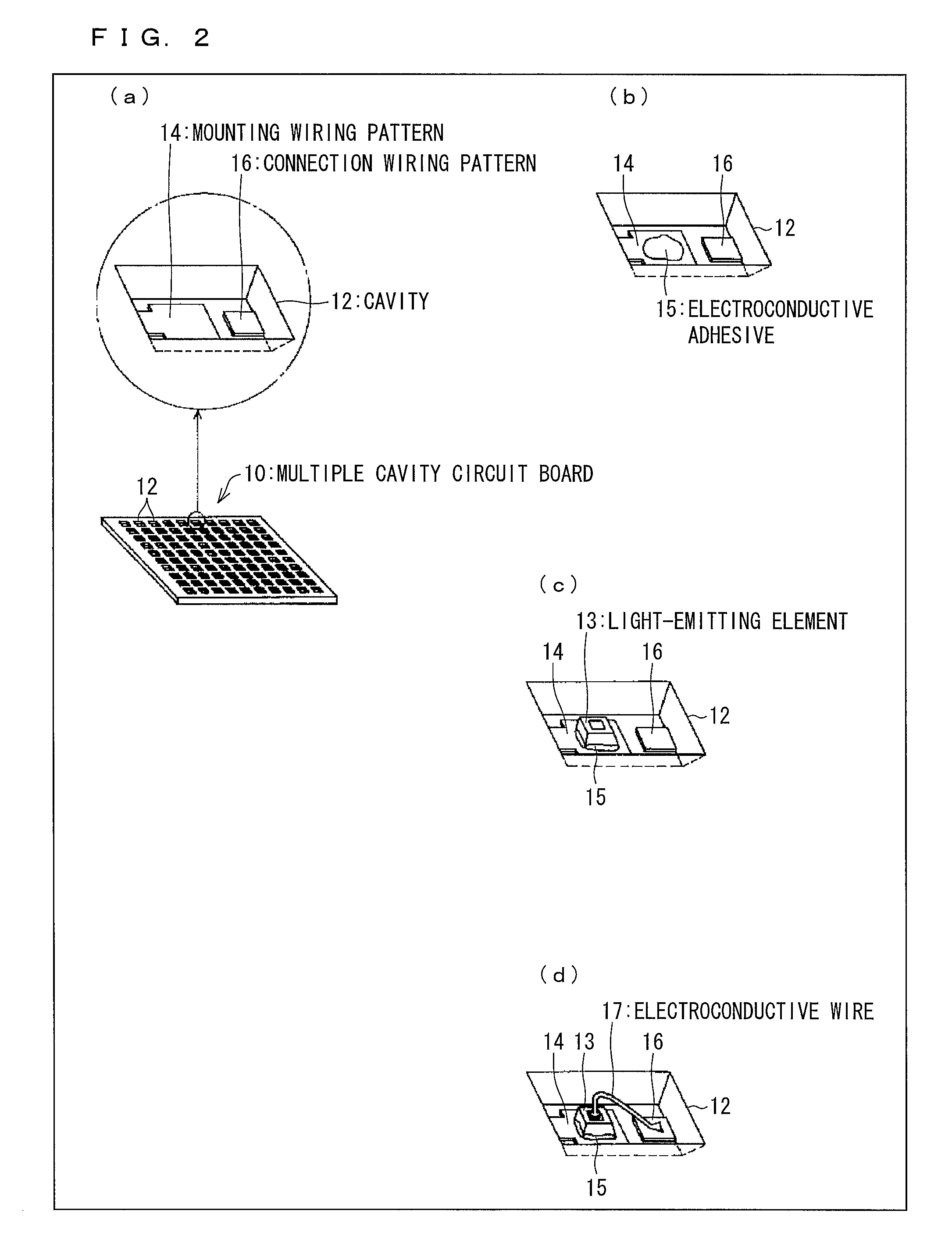
Figure 3
Abstract
Description
CROSS-REFERENCE TO RELATED APPLICATIONS
[0001] This application is a national stage application under 35 USC 371 of International Application No. PCT / JP2012 / 066174, filed Jun. 25, 2012, which claims the priority of Japanese Applications No. 2011-260936, filed Nov. 29, 2011, and 2012-019150, filed Jan. 31, 2012, the contents of which prior applications are incorporated herein by reference.FIELD OF THE INVENTION
[0002] The present invention relates to a method for producing a light-emitting device in which a fluorescent material is used.BACKGROUND OF THE INVENTION
[0003] A light-emitting device in which an LED chip and a fluorescent material are used, the fluorescent material emitting fluorescence by being excited by light emission by the LED chip, is classified into the following known types according to how to provide the fluorescent material in a vicinity of the LED chip.
[0004] The known types include a two-stage sealing type (Patent Literature 1) in which an LED chip 151 is sealed by car...