High speed bypass cable assembly

a high-speed, bypass cable technology, applied in the direction of cables, non-printed jumper connections, coupling device connections, etc., can solve the problems of high-speed applications that cannot be used with fr-4 materials, increase the cost of circuit boards, and the price of these materials is severely increased. , to achieve the effect of low loss characteristics

Active Publication Date: 2015-04-21
MOLEX INC
View PDF15 Cites 119 Cited by
  • Summary
  • Abstract
  • Description
  • Claims
  • Application Information

AI Technical Summary

Benefits of technology

[0005]Accordingly, there is provided an improved high speed bypass cable assembly that defines a signal transmission line useful for high speed applications at 10 GHz or above and with low loss characteristics.
[0007]In accordance with a second embodiment of the disclosure, the cable bypass assembly provides a transmission line that is separate from the circuit board, and may include one or more associated signal wire pairs, such as is found in “twin-ax” cable. The wires of the bypass cable are configured at their opposite ends in two fashions. At a first end of the bypass cable, the wires are configured for a direct termination to a board mounted connector, and are arranged in a manner such that the conductors of the signal wires extend in alignment with terminal termination ends, or feet, of the board mounted connector. The shielding of the signal wires are rolled back upon the insulative coating of the wires and exterior shield extensions are preferably provided to ensure that the signal wire conductor leads are effectively shielded through the connection. In this manner of connection, the terminal tails need not be attached to the circuit board, either as surface mount or through hole tails, thereby significantly reducing losses and the impedance discontinuity that occurs in the tail to board mounting transition.
[0008]At the second end of the bypass cable the signal wires are terminated in a fashion so that they can either be connected directly to the chip member or to the board in close proximity to the chip member. In this regard, and as disclosed in this second embodiment, the signal wire conductors are terminated to associated tail portions that are aligned with the conductors, similar to the termination which occurs at the first end. These tails are maintained in a desired spacing and are further completely shielded by a surrounding conductive enclosure to provide full EMI shielding and reduction of cross talk. The termination of the ends of the bypass cable assembly are done in a manner such that to the extent possible, the geometry of the conductors in the bypass cable is maintained through the termination of the cable to the board connector and / or the chip.

Problems solved by technology

However, FR-4 is known to promote losses in high speed signal transmission lines, and these losses make it undesirable to utilize FR-4 material for high speed applications (10 GHz and above).
Custom materials for circuit boards are available that reduce such losses but the price of these materials severely increase the cost of the circuit board and, consequently, the electronic devices in which they are used.
These long lengths require that the signals traveling through the transmission line be amplified and repeated, thereby increasing the cost of the circuit board, and complicating the design inasmuch as additional board space is needed to accommodate these amplifiers and repeaters.
In addition, the routing of the traces of such a transmission line in the FR-4 may require multiple turns and the transitions which occur at terminations affect the integrity of the signals transmitted thereby.
It becomes difficult to route transmission line traces in a manner so as to achieve consistent impedance and a low signal loss therethrough.

Method used


Image

  • High speed bypass cable assembly
  • High speed bypass cable assembly
  • High speed bypass cable assembly

Examples


Embodiment Construction

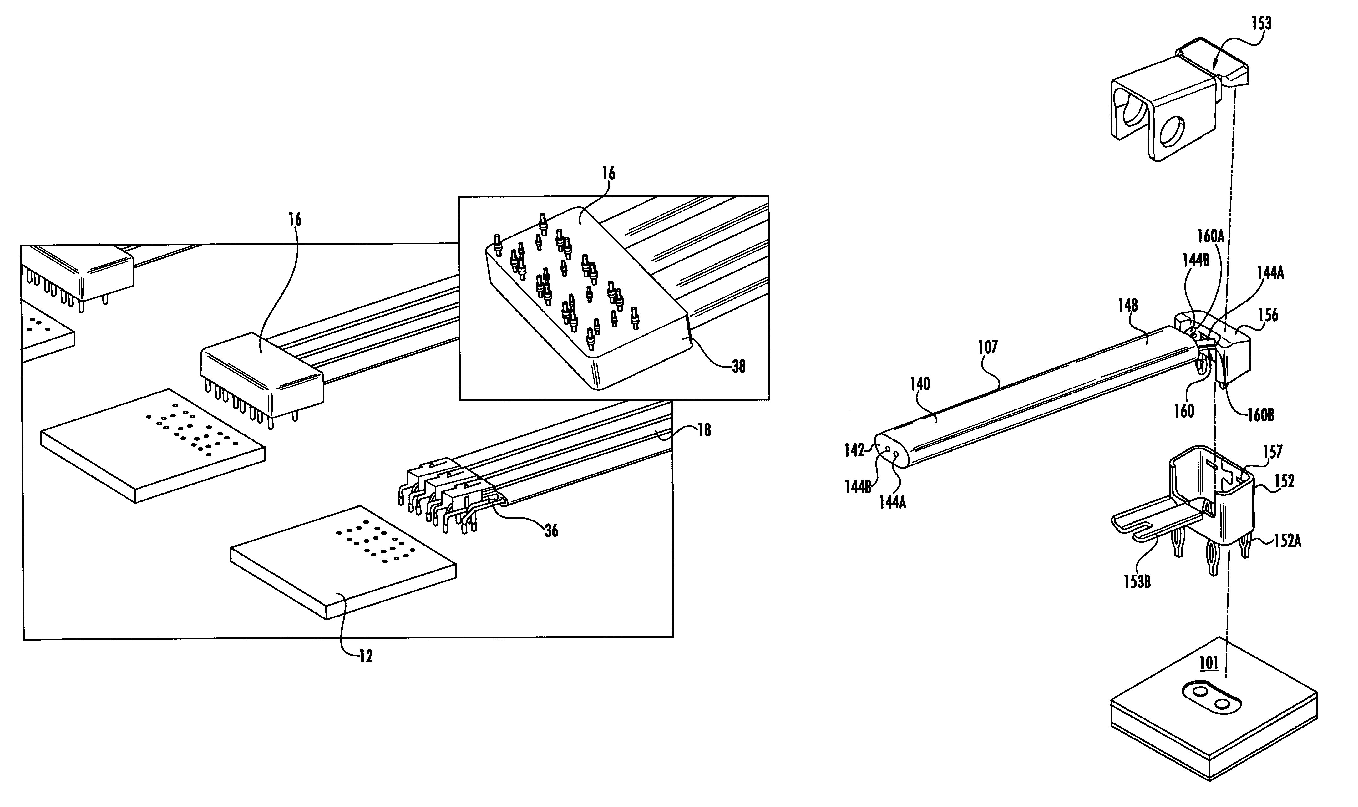
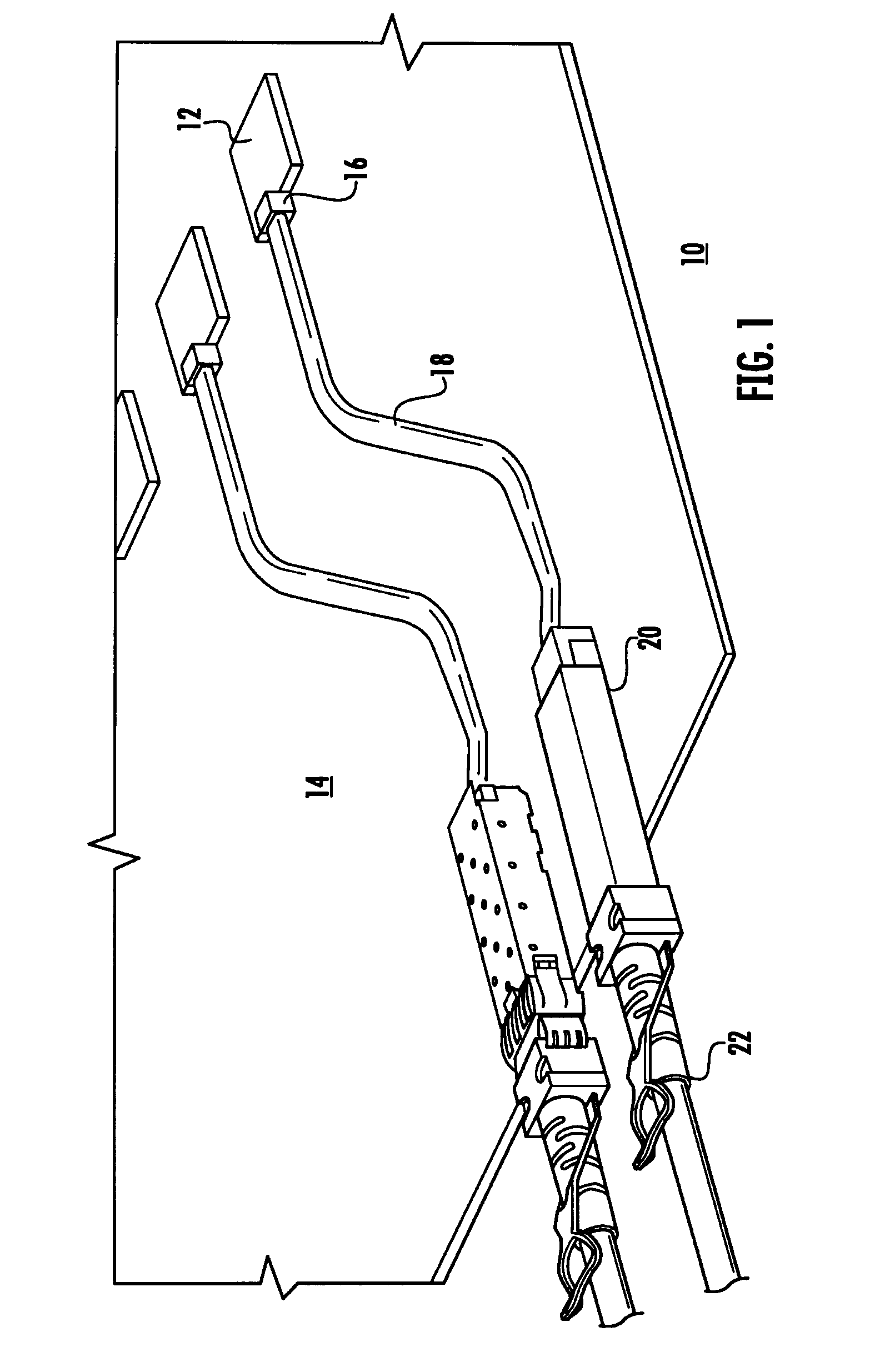
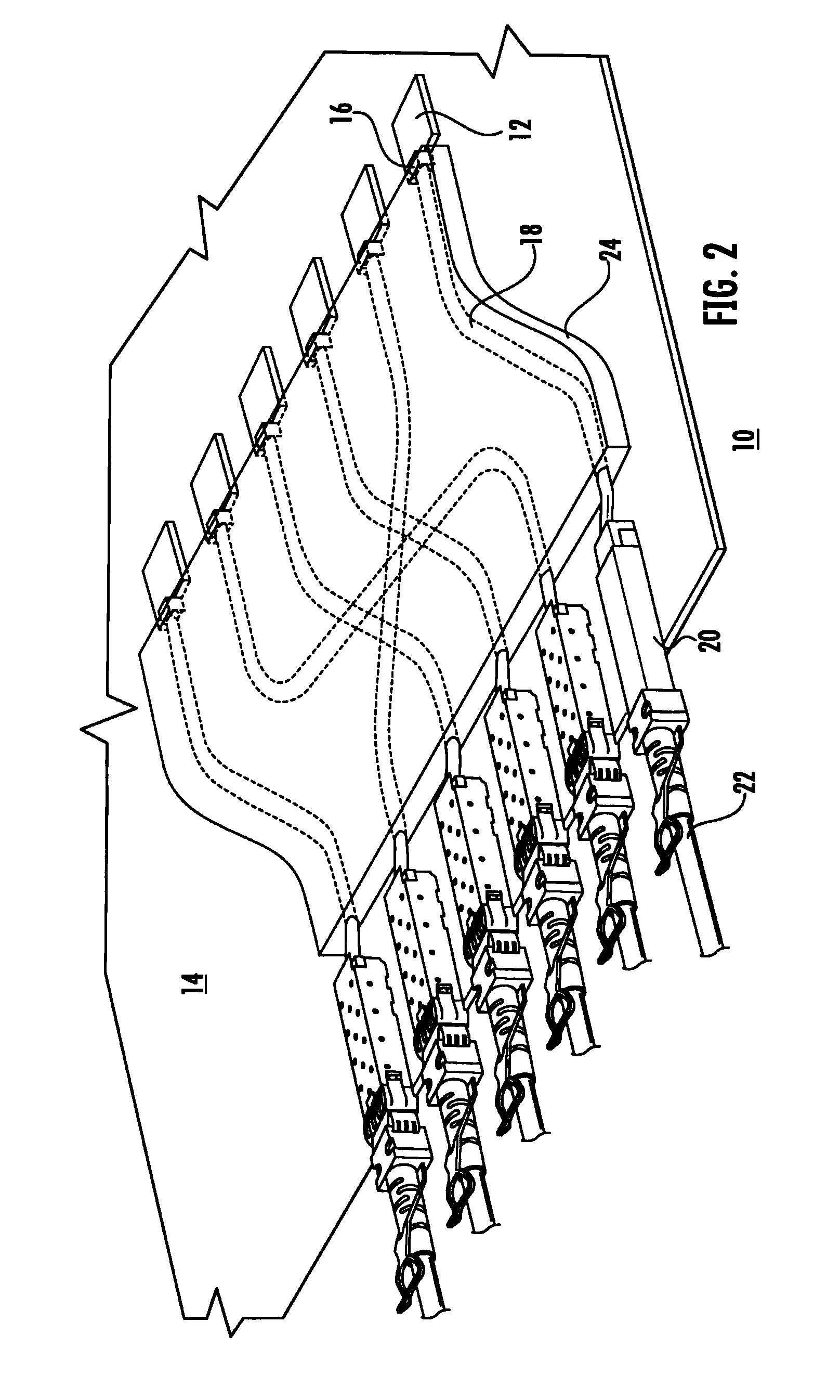
[0037]While the Present Disclosure may be susceptible to embodiment in different forms, there is shown in the Figures, and will be described herein in detail, specific embodiments, with the understanding that the disclosure is to be considered an exemplification of the principles of the Present Disclosure, and is not intended to limit the Present Disclosure to that as illustrated.

[0038]In the embodiments illustrated in the Figures, representations of directions such as up, down, left, right, front and rear, used for explaining the structure and movement of the various elements of the Present Application, are not absolute, but relative. These representations are appropriate when the elements are in the position shown in the Figures. If the description of the position of the elements changes, however, these representations are to be changed accordingly.

[0039]While the Present Disclosure may be susceptible to embodiment in different forms, there is shown in the Figures, and will be des...


PUM

PropertyMeasurementUnit
lengthaaaaaaaaaa
frequencyaaaaaaaaaa
frequencyaaaaaaaaaa

Abstract

A cable bypass assembly is disclosed for use in providing a high speed transmission line for connecting a board mounted connector of an electronic device to a chip on the device board. The bypass cable assembly has a structure that permits it, where it is terminated to the board mounted connector and the chip member, or closely proximate thereto to replicate closely the geometry of the cable. The connector terminals are arranged in alignment with the cable signal conductors and shield extensions are provided so that shielding can be provided up to and over the termination between the cable signal conductors and the board connector terminal tails. Likewise, a similar termination structure is provided at the opposite end of the cable where a pair of terminals are supported by a second connector body and enclosed in a shield collar. The shield collar has an extension that engages the second end of the cable.

Description

REFERENCE To RELATED APPLICATIONS[0001]The Present Disclosure is a continuation-in-part of International Application No. PCT / US2010 / 022738, filed Feb. 1, 2010, entitled “High Speed Interconnect Cable Assembly,” filed 01 Feb. 2010 with the U.S. Patent And Trademark Office (USPTO) as Receiving Office for the Patent Cooperation Treaty. The '738 Application claims priority of prior-filed U.S. Provisional Application No. 61 / 145,685, entitled “High Speed Interconnect Cable Assembly,” filed 30 Jan. 2009 also with the USPTO. The contents of each of the above Applications are fully incorporated in their entireties herein.BACKGROUND OF THE PRESENT DISCLOSURE[0002]The Present Disclosure relates generally to cable interconnection systems, and more particularly, to bypass cable interconnection systems for transmitting high speed signals at low losses.[0003]Conventional cable interconnection systems are found in electronic devices such as routers and servers and the like, and are used to form a s...

Claims


Application Information

Patent Timeline
Patent Type & Authority Patents(United States)
IPC IPC(8): H01R13/58H01B11/00H01R13/6593H05K1/02H05K3/22
CPCH01B11/00H01R13/6593H05K1/0243H05K3/222H05K2201/10189H05K2201/10356H05K2201/10446H05K2201/10674H01R13/6471H01R13/6461H01R13/6592
Inventor LLOYD, BRIAN KEITHHIRSCHY, CHRISTOPHER DAVIDAHMAD, MUNAWARJONES, ERAN J.HAMBLIN, STEPHEN W.SCHULZ, DARIAN ROSSWARD, TODD DAVIDWALZ, GREGORY B.ABUNASRAH, EBRAHIMKHAN, REHAN M.
Owner MOLEX INC
Why Eureka
Try Eureka