Plastic photonic crystal fiber for terahertz wave transmission and method for manufacturing thereof
a technology of terahertz wave transmission and photonic crystal fiber, which is applied in the direction of optical waveguide light guide, instruments, optics, etc., can solve the problems of difficult to produce a physically flexible thz waveguide by using those materials, and the problem of silica pcf also revealing the same problems, so as to achieve easy fabrication, low loss characteristic, and cost-effective
- Summary
- Abstract
- Description
- Claims
- Application Information
AI Technical Summary
Benefits of technology
Problems solved by technology
Method used
Image
Examples
second embodiment
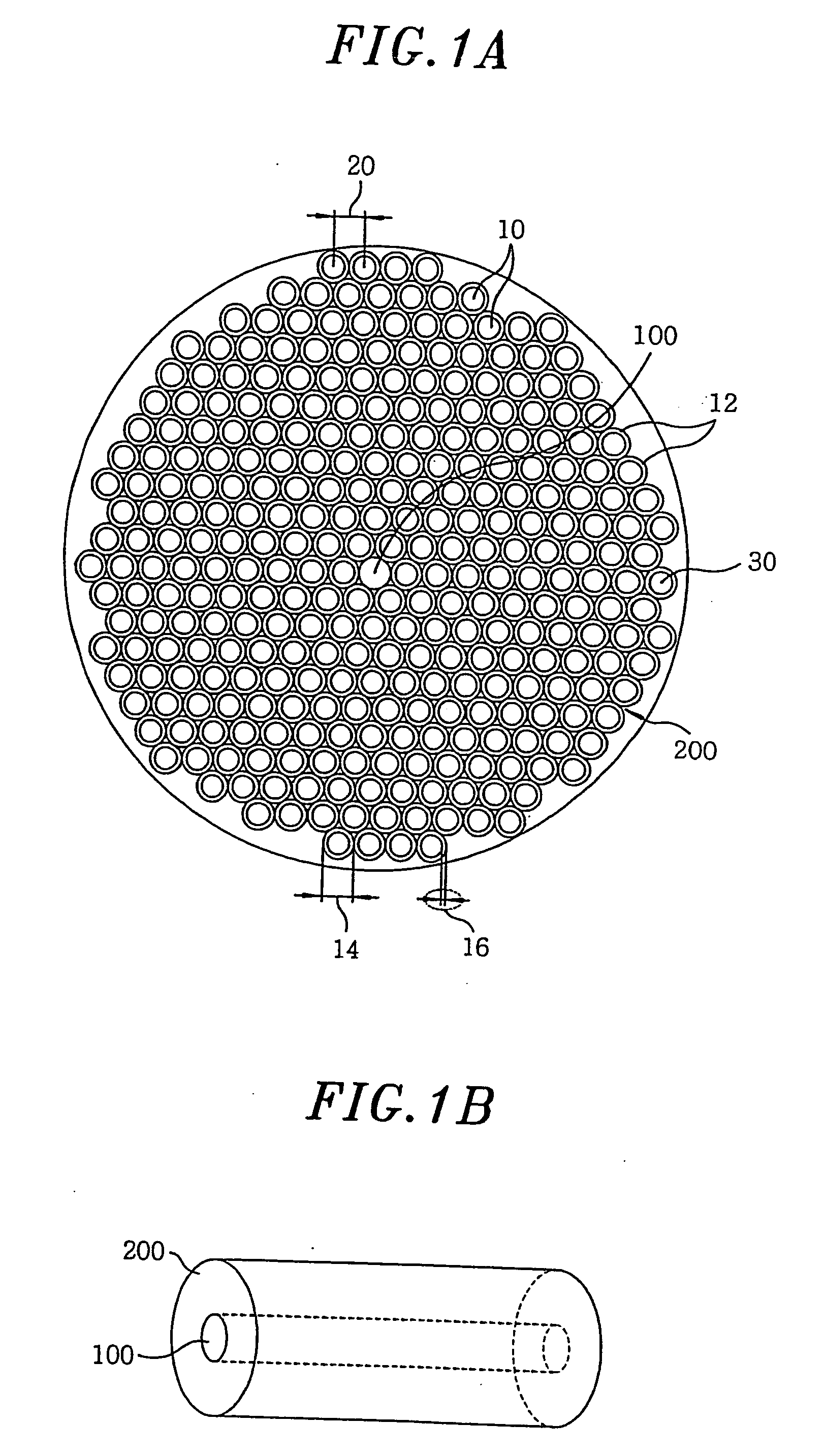
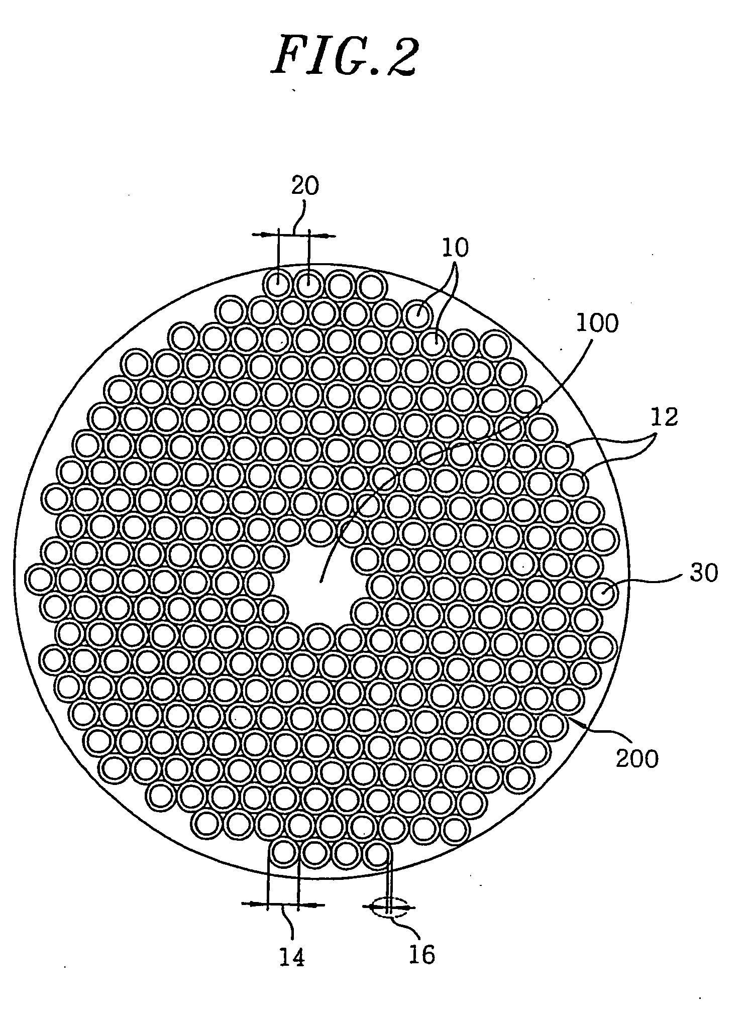
[0063] Referring to FIG. 2, there is provided a PPCF in accordance with a second preferred embodiment of the present invention. The PPCF of the second embodiment also includes the crystal defect component 100 and the photonic crystal component 200, and the photonic crystal component 200 is arranged to form a 2D photonic crystal structure having a predetermined lattice constant.
[0064] The photonic crystal component 200 in the second embodiment is identical to the one explained in the first preferred embodiment of FIG. 1. Thus, a detailed description of the photonic crystal component 200 will be omitted. However, the crystal defect component 100 in the second embodiment is different from the one used in the first preferred embodiment in some respects. First, a guiding mechanism using the photonic band gap effect is employed to perform an optical transmission, unlike in the first embodiment. Further, the crystal defect component 100 is preferably prepared by taking out from the crystal...
third embodiment
[0067] Referring to FIG. 4, there is depicted a block diagram describing a process for fabricating a PPCF in accordance with the present invention. First, a crystal defect component member is prepared to temporarily fill the crystal defect component 100 having a predetermined diameter (Step 10). Such crystal defect component member is, for example, a tube or a filament. Next, a plurality of plastic elements 30 having a predetermined diameter is prepared (Step 20) and the prepared plastic elements 30 are, then, arranged to surround the crystal defect component member, i.e., the tube and the filament, forming a 2D photonic crystal structure having a predetermined lattice constant (Step 30). Thereafter, a heat-treatment is performed in a manner that the neighboring plastic elements 30 are attached to each other but the crystal defect component 100 and its ambient plastic elements are not stuck to each other (Step 40). Then, the crystal defect component member used to temporarily fill t...
PUM
 Abstract
Description
Claims
Application Information


