Filter having switch function and band pass filter

a filter and function technology, applied in the direction of resonators, electrical equipment, waveguides, etc., can solve the problems of increased filter transmission loss, easy increase of device costs, circuit transmission loss, etc., and achieve low cost, low loss characteristic, and reduced number of components

Inactive Publication Date: 2011-12-06
NEC CORP +1
View PDF11 Cites 20 Cited by
  • Summary
  • Abstract
  • Description
  • Claims
  • Application Information

AI Technical Summary

Benefits of technology

[0010]In view of the foregoing, it is an object of the present invention to provide a filter having a switch function and a band pass filter which can obtain a low loss characteristic at low costs while making possible reduction in the number of components.
[0012]In the filter having the switch function, electrical conductivity in a region between the neighborhood of the open end of the inner conductor and the metal case are switched between a conductive state and a non-conductive state, so that the frequency characteristic of the branch waveguide can be changed, and a switch can be configured using the frequency characteristic. Accordingly, a switch construction and a filter construction can be integrated, so that the number of components or miniaturization of a device can be achieved. Also, since a resonator is not disposed on a plane circuit as in a conventional filter having a switch function, a low loss filter can also be realized.
[0013]In the filter having the switch function, the short-circuiting portion may be configured to include a short-circuiting plate constructed between the neighborhood of the open end of the inner conductor and the metal case, a short circuit line disposed on the short-circuiting plate to electrically connect the neighborhood of the open end of the inner conductor with the metal case, and an active device disposed on the short circuit line to switch, between a conductive state and a non-conductive state, electrical conductivity in a region between the neighborhood of the open end of the inner conductor and the metal case. According to this construction, a conduction state between the neighborhood of the open end of the inner conductor and the metal case may be easily switched, and simultaneously, a switch may be configured with a simple construction.
[0014]In the filter having the switch function, the short-circuiting plate may be integrally formed with a stacked print substrate installed between the metal case and a metal cover. According to this construction, only the short-circuiting plate does not need to be separately formed. Also, even when the short-circuiting plate is attached inside the metal case, an attaching process may be completed simultaneously with attachment of the stacked print substrate, so that the number of components or assembling manhours may be reduced.
[0016]In the filter having the switch function, the conductive plate may be formed by attaching a conductive coated film on a surface of a dielectric plate integrally formed with the stacked print substrate, and the short-circuiting portion may allow the conductive coated film to be selectively conducted to the metal case. Accordingly, the number of components or assembling manhours may be reduced.
[0019]As described above, it is possible to provide the filter having a switch function that can obtain a low loss characteristic at low costs while making possible reduction in the number of components.

Problems solved by technology

However, since the number of electrical and mechanistic components increases in this case, device costs may easily increase, and also, a transmission line of RF signals is lengthened, which increases a transmission loss of the circuit.
However, since the filter circuit has a construction of mounting a circuit device such as a chip condenser and a resonator on a plane circuit, that is, a plate-shaped dielectric substrate, and connecting the circuit device on a microstrip line, the transmission loss of the filter may be increased by the dielectric loss of the dielectric substrate.
An increase in the transmission loss of the filter causes an increase of power consumption in a transmission circuit of a wireless device, and also, is directly connected with deterioration of a noise figure (NF) in a reception circuit.
In that case, use of a low-loss substrate can be considered, but such a substrate is expensive.
Also, when a low-cost substrate is used, selectivity of a material is not sufficient, so that it is difficult to obtain desired characteristics.

Method used


Image

  • Filter having switch function and band pass filter
  • Filter having switch function and band pass filter
  • Filter having switch function and band pass filter

Examples


first embodiment

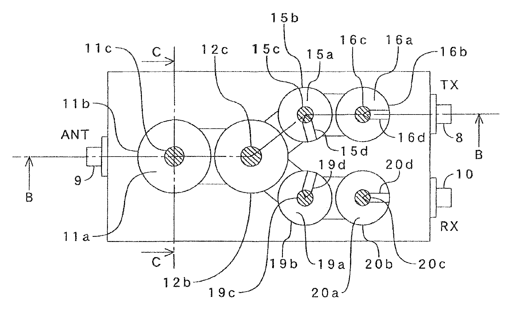
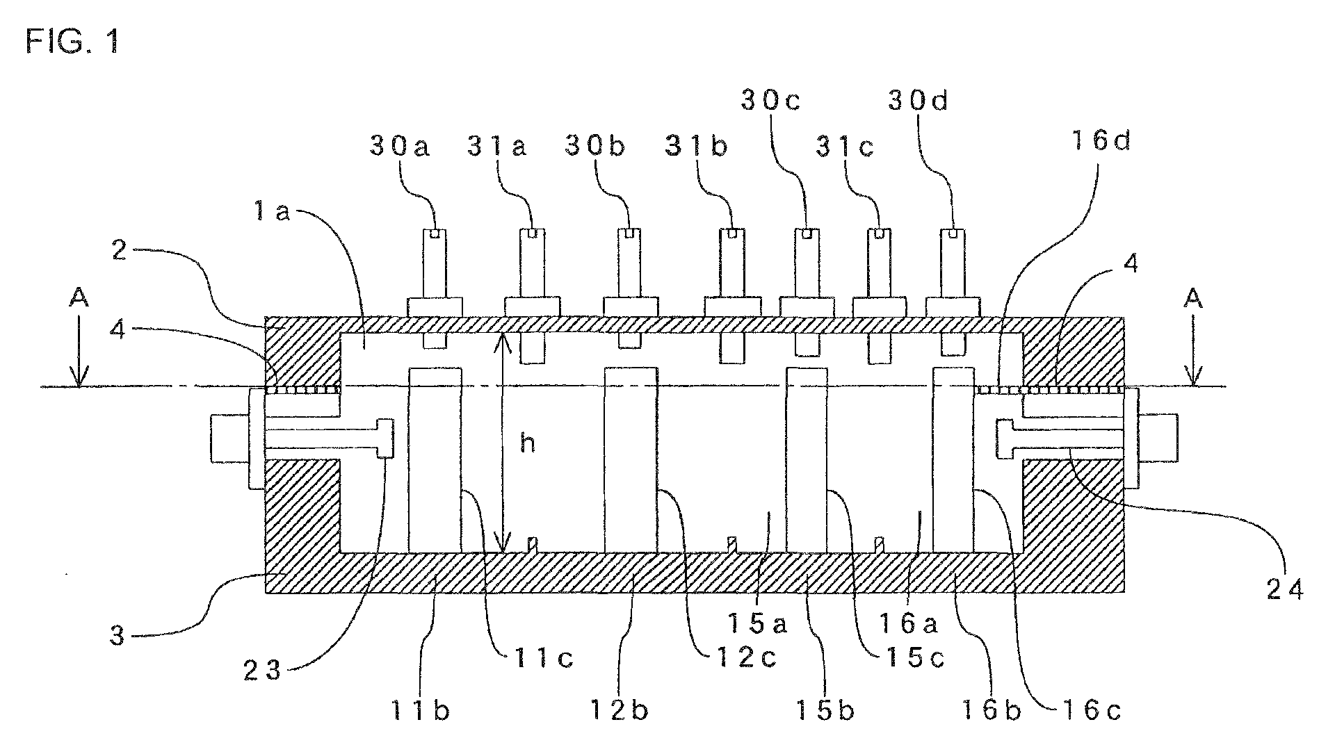
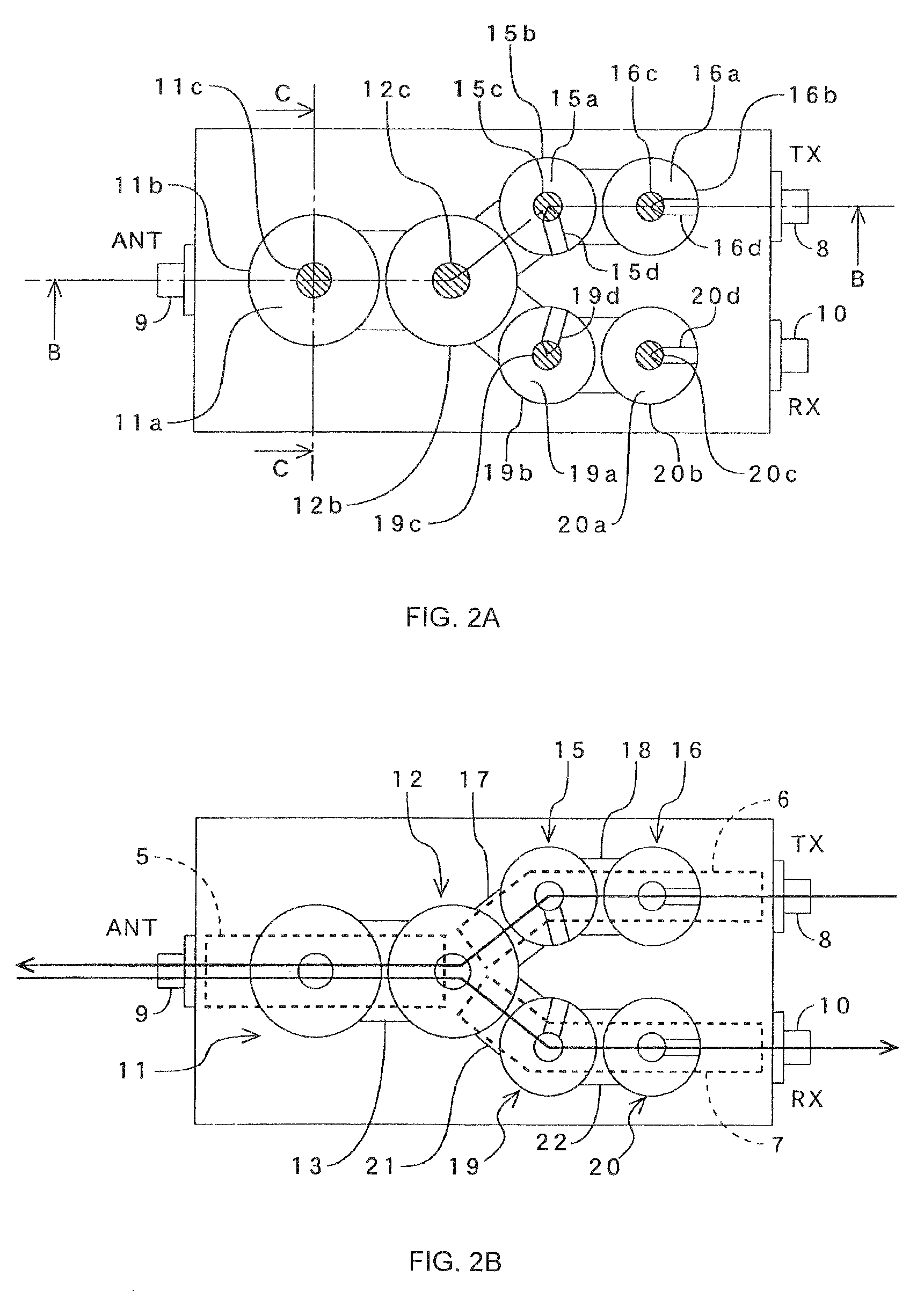
[0048]FIGS. 1 to 3 are construction view illustrating a filter having a switch function according to the present invention. Also, FIG. 1 is a cross-sectional view taken along a line B-B of FIGS. 2A and 2B, FIGS. 2A and 2B are cross-sectional views taken along a line A-A of FIG. 1, and FIG. 3 is a cross-sectional view taken along a line C-C of FIGS. 2A and 2B.

[0049]As illustrated in FIG. 1, a filter 1 having a switch function roughly includes a metal case 2, a metal cover 3 covered with the metal case 2, and a stacked print substrate 4 inserted between the metal case 2 and the metal cover 3. A space 1a having a height h equal to or less than a wavelength λ / 4 of a use frequency and having a Y-shape (refer to FIG. 2A) as viewed from above is formed inside the metal case 2 and the metal cover 3. As illustrated in FIG. 2B, a primary waveguide 5, and first and second branch waveguides 6 and 7 branching from the primary waveguide 5 are formed.

[0050]The primary waveguide 5 is a transmission...

second embodiment

[0069]Next, the filter having the switch function according to the present invention is described with reference to FIGS. 18 to 21.

[0070]Since an electric field has a maximum value in the neighborhood of the open end of the central conductor, but the PIN diodes on the substrate are grounded from the outer conductor to the central conductor in an RF manner in the filter 1 having the switch function illustrated in FIGS. 1 to 14, a potential difference of an RF between both ends of the PIN diode increases. For this reason, when an RF signal of 1 W or more is transmitted from a transmission side to the filter, the RF signal exceeds the rated power of the PIN diode, so that there is possibility that transmittable power may be limited.

[0071]The filter having the switch function according to an embodiment has improved power-withstanding property of a transmission side, and is illustrated in FIGS. 18 and 19. Also, FIG. 18B is a cross-sectional view taken along a line G-G of FIG. 18A, and FI...


PUM


Abstract

The filter has a switch function of selectively transmitting a transmission signal through one of first and second branch waveguides branching from a primary waveguide. The filter includes resonators disposed in the first and second branch waveguides. The resonator includes a space formed inside a metal cover, a central conductor disposed inside the space, and a short-circuiting plate. The central conductor has one end grounded to an outer conductor. The short-circuiting plate allows the neighborhood of an open end of the central conductor to be selectively conducted to the outer conductor. The filter performs a selection from the first and second branch waveguides by switching electrical conductivity in a region between the neighborhood of the open end of the central conductor and the outer conductor.

Description

[0001]This application is based on Japanese patent application No. 2007-324156, the content of which is incorporated herein by reference.BACKGROUND[0002]1. Technical Field[0003]The present invention relates to a filter having a switch function and a band pass filter, and more particularly, to a filter having a switch function suitable for a radio frequency (RF) communication device used in common for an antenna in a base station for a cellular phone adopting time division duplex scheme.[0004]2. Related Art[0005]Conventionally, a RF communication device used in common for an antenna by time division duplex scheme realizes transmission of baseband signals by switching between a transmission circuit and a reception circuit through time division using the same frequency band. In this kind of RF communication device, an RF switch circuit 74 having a construction of single pole double throw (SPDT) is installed between transmission / reception circuits (TX circuit 71 and RX circuit 72) and a...

Claims


Application Information

Patent Timeline
Patent Type & Authority Patents(United States)
IPC IPC(8): H01P5/12H01P1/20
CPCH01P1/2133H01P1/2136H01P7/10H01P1/20
Inventor TANPO, HIROSHIHAMADA, TSUYOSHI
Owner NEC CORP
Why Eureka
Try Eureka