Method for manufacturing electronic grade synthetic quartz glass substrate

a technology of electronic grade and synthetic quartz glass, which is applied in the direction of manufacturing tools, originals for photomechanical treatment, instruments, etc., can solve the problems of focal shift or pattern shift risk, and achieve the effect of minimizing the change of shape factor and high accuracy of shape factor

Active Publication Date: 2015-04-28
SHIN ETSU CHEM IND CO LTD
View PDF28 Cites 0 Cited by
  • Summary
  • Abstract
  • Description
  • Claims
  • Application Information

AI Technical Summary

Benefits of technology

[0025]In the manufacture of an electronic grade synthetic quartz glass substrate having a recess, channel or step, for example, a synthetic quartz glass substrate for use as a photomask substrate in the photolithography or a mold substrate in the nanoimprint lithography (NIL) for the fabrication of IC and other electronic devices, the method of the invention is able to produce a glass substrate having a high accuracy of shape factor in a relatively simple manner by providing a glass substrate having a maximum birefringence within a certain range in its entirety, machining the substrate to form a recess, channel or step therein, and removing the residual stress due to machining, specifically by mirror finish polishing or wet etching to remove a work affected layer in the machined surface. The substrate as a whole experiences a minimized change of shape factor before and after formation of the recess, channel or step.

Problems solved by technology

If the substrate whose surface has experienced substantial changes of flatness and parallelism is used in the photomask or NIL application without readjustment, there is a risk of a focal shift occurring upon exposure or a pattern shift occurring upon transfer.

Method used


Image

  • Method for manufacturing electronic grade synthetic quartz glass substrate
  • Method for manufacturing electronic grade synthetic quartz glass substrate
  • Method for manufacturing electronic grade synthetic quartz glass substrate

Examples


example 1

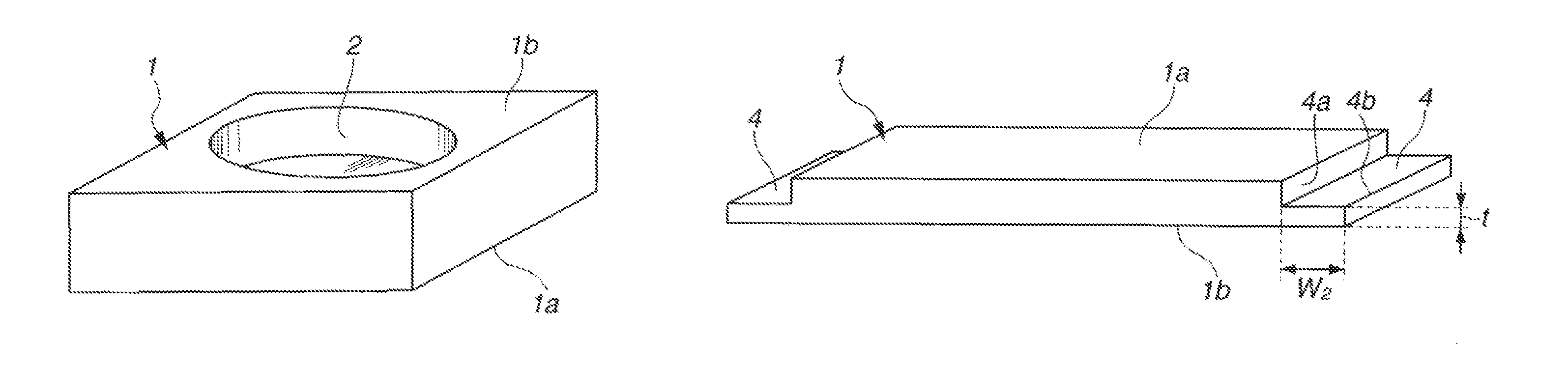
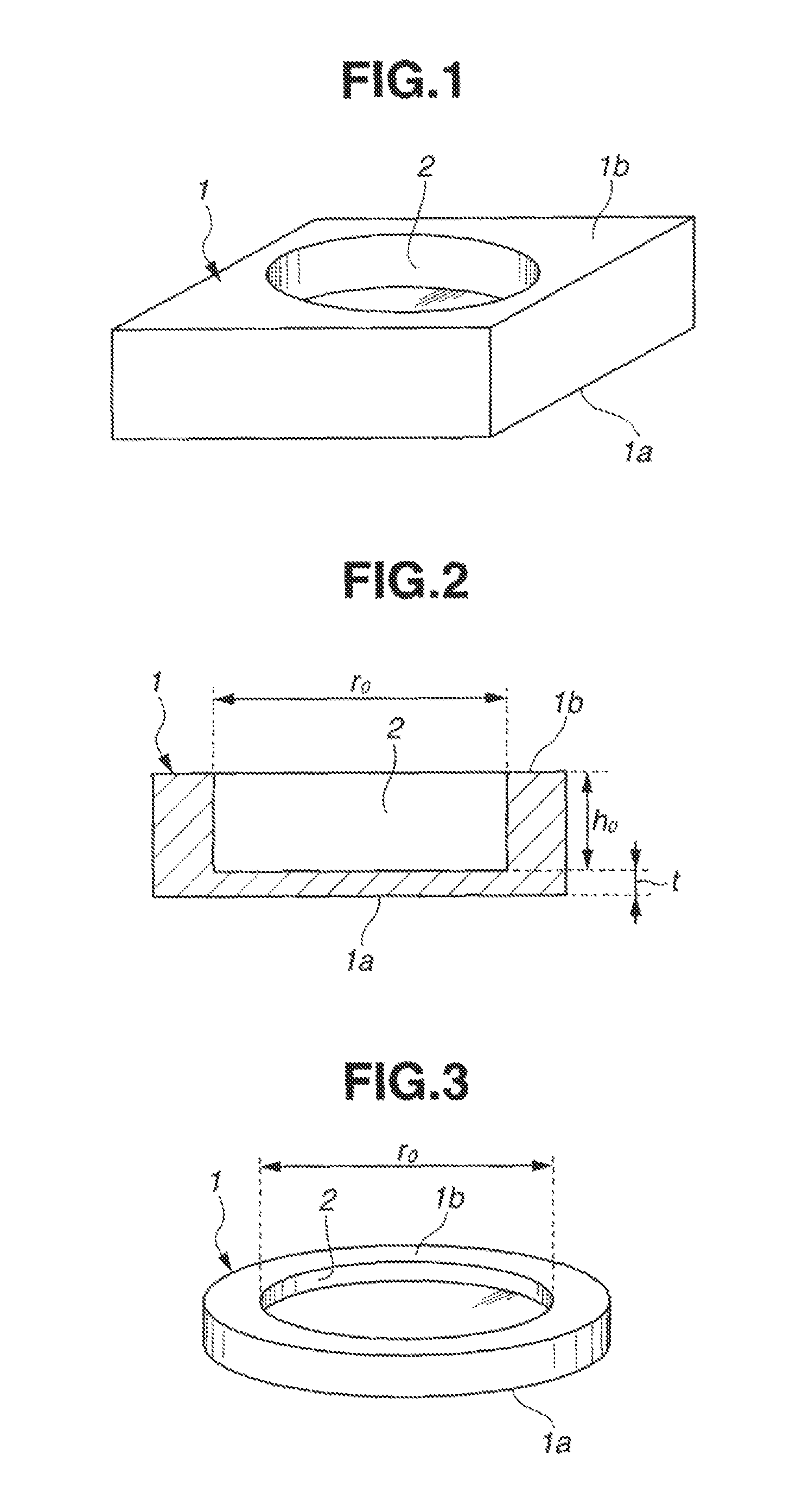
[0079]A synthetic quartz glass substrate dimensioned 100 mm×100 mm×6.35 mm (thick) having front, back and end surfaces polished to mirror finish was prepared as a starting substrate. The starting substrate had a maximum birefringence of 0.93 nm / cm in its entirety, the front surface of the substrate in a central region of 90 mm×90 mm had a flatness of 0.091 μm, the back surface in a region excluding a center circle with a diameter of 70 mm had a lo flatness of 0.121 μm, and the substrate excluding a center circle with a diameter of 70 mm had a parallelism of 0.3 μm. Using a machining center and a diamond abrasive wheel, the starting substrate was machined at the center of its back surface to form a circular recess having a depth of 5.32 mm and a diameter of 69.98 mm.

[0080]Next, the machined substrate was fixedly mounted on a platform. A wool felt buff having a diameter of 50 mm and a height of 30 mm adapted to rotate at 1,000 rpm was forced in contact with the bottom surface of the r...

example 2

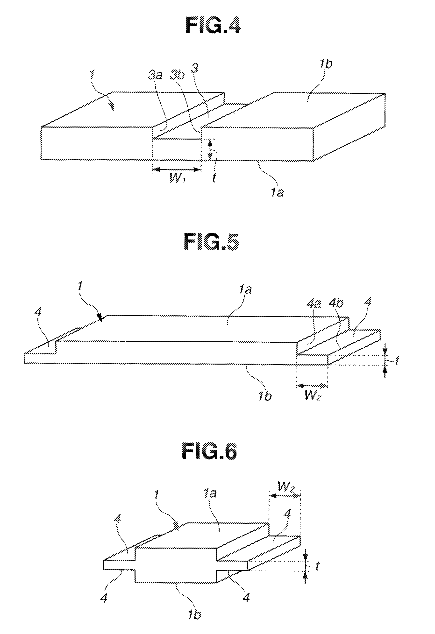
[0082]A synthetic quartz glass substrate dimensioned 152 mm×152 mm×6.35 mm (thick) having front, back and end surfaces polished to mirror finish was prepared as a starting substrate. The starting substrate had a maximum birefringence of 1.53 nm / cm in its entirety, the front surface of the substrate in a central region of 142 mm×142 mm had a flatness of 0.235 μm, the back surface in a region excluding a central region of 152 mm×30 mm had a flatness of 0.481 μm, and the substrate excluding a central region of 142 mm×30 mm had a parallelism of 0.9 μm. Using a machining center and a diamond abrasive wheel, the starting substrate was machined at the center of its back surface to form a channel having a depth of 4.98 mm, a width of 29.98 mm and a length of 152 mm, extending parallel to the end surface.

[0083]Next, the machined substrate was fixedly mounted on a platform. A wool felt buff having a diameter of 30 mm and a height of 30 mm adapted to rotate at 1,000 rpm was forced in contact w...

example 3

[0085]A synthetic quartz glass substrate dimensioned 200 mm×400 mm×10 mm (thick) having front, back and end surfaces polished to mirror finish was prepared as a starting substrate. The starting substrate had a maximum birefringence of 2.43 nm / cm in its entirety, the front surface of the substrate in a central region of 190 mm×390 mm had a flatness of 2.303 μm, the back surface in a central region of 190 mm×360 mm had a flatness of 3.145 μm, and the substrate in a central region of 190 mm×360 mm had a parallelism of 5.3 μm. Using a machining center and a diamond abrasive wheel, the starting substrate was machined on its back surface along both ends to form steps having a depth of 6.95 mm, a width of 19.99 mm and a length of 200 mm, extending parallel to the end surface.

[0086]Next, the machined substrate was fixedly mounted on a platform. A wool felt buff having a diameter of 30 mm and a height of 30 mm adapted to rotate at 1,000 rpm was forced in contact with the bottom surface of th...


PUM

PropertyMeasurementUnit
pressureaaaaaaaaaa
flatnessaaaaaaaaaa
flatnessaaaaaaaaaa

Abstract

An electronic grade synthetic quartz glass substrate having a recess, channel or step is manufactured by machining at least one surface of a synthetic quartz glass substrate having a maximum birefringence of up to 3 nm / cm in its entirety to form a recess, channel or step, and removing the residual stress due to machining.

Description

CROSS-REFERENCE TO RELATED APPLICATION[0001]This non-provisional application claims priority under 35 U.S.C. §119(a) on Patent Application No. 2010-146507 filed in Japan on Jun. 28, 2010, the entire contents of which are hereby incorporated by reference.TECHNICAL FIELD[0002]This invention relates to a method for manufacturing electronic grade synthetic quartz glass substrates having a recess, channel or step and more particularly, a method for manufacturing synthetic quartz glass substrates for use in the advanced applications of semiconductor-related electronic materials, typically as photomasks, exposure tool components, reticles and nanoimprint molds.BACKGROUND ART[0003]The quality of synthetic quartz glass substrates is evaluated in terms of the size and population of defects on the substrate, flatness, surface roughness, photochemical stability of material, and surface chemical stability. The trend toward higher accuracy of the design rule poses ever-tightening requirements on ...

Claims


Application Information

Patent Timeline
Patent Type & Authority Patents(United States)
IPC IPC(8): B24B7/24B24B7/22B24B19/03C03C15/02
CPCB24B7/241C03C15/02B24B19/03B24B7/228G03F1/60H01L21/0274
Inventor OKAFUJI, DAIYUTAKEUCHI, MASAKIYAMAZAKI, HIROYUKI
Owner SHIN ETSU CHEM IND CO LTD
Why Eureka
Try Eureka